Method for filtering nuisance defects

a technology of nuisance defects and filtering methods, applied in the field of detecting defects in fabricated wafers, can solve the problems of reducing die performance and performance reduction

Active Publication Date: 2006-06-01
APPL MATERIALS ISRAEL LTD
View PDF18 Cites 31 Cited by
  • Summary
  • Abstract
  • Description
  • Claims
  • Application Information

AI Technical Summary

Benefits of technology

[0011] In embodiments of the present invention, a wafer inspection system generates a set of defects of the wafer, and the system performs an initial filtration of the defects to generate candidate defects for further analysis. The inspection system generates values of image attributes for each of the candidate defects, the image attributes typically comprising expressions that are functions of measurements of the candidate defects made by the inspection system. The image attributes may be generated from one or more signals from the candidate defects.

Problems solved by technology

One of the problems of defect identification is that identified defects may in fact not lead to reduced performance of the die.
For example, the existence of metal grains in the die, of a rough edge on a conductor, or of anomalies under a scanned layer, typically do not reduce performance.

Method used


Image

  • Method for filtering nuisance defects
  • Method for filtering nuisance defects
  • Method for filtering nuisance defects

Examples


Embodiment Construction

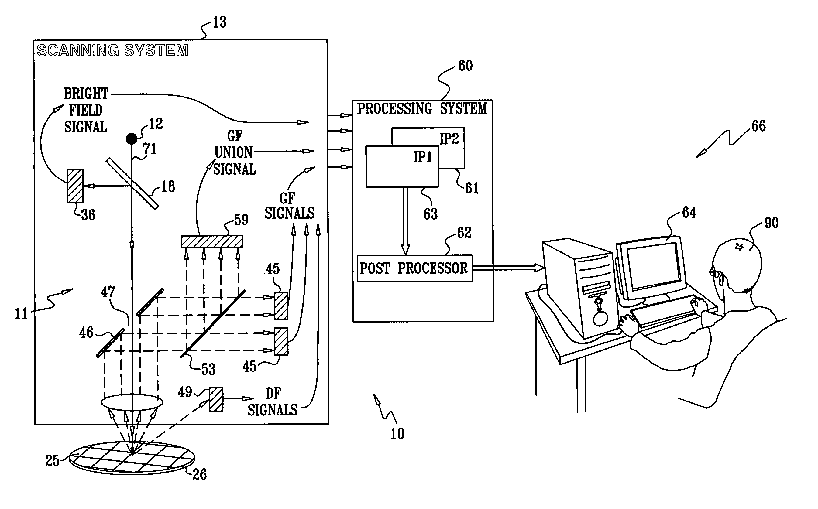
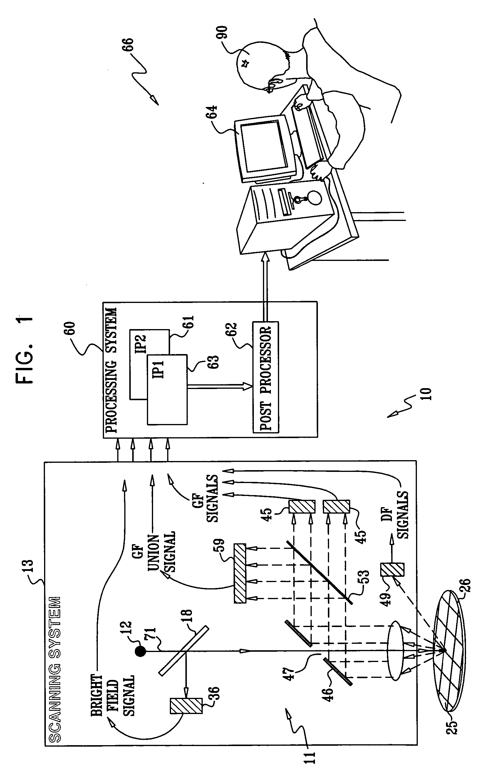
[0021] Reference is now made to FIG. 1, which is a schematic illustration of a wafer inspection apparatus 10, according to an embodiment of the present invention. Apparatus 10 is used to inspect a surface 25 of a wafer 26, typically a semiconductor wafer, during one or more stages of fabrication of the wafer. Herein, by way of example, apparatus 10 is assumed to use an optical inspection scanning system 13, but those having ordinary skill in the art will be able, mutatis mutandis, to adapt the following description to accommodate other inspection systems or combinations of inspection systems. Such systems include, but are not limited to, inspection of wafer 26 by substantially any type of electromagnetic radiation and / or charged particle scanning.

[0022] Apparatus 10 comprises a source 12, typically a laser, which radiates an optical beam 71 onto surface 25. Reflected and / or scattered light that results from the irradiation is detected in a number of detectors 11. Herein detectors 1...


PUM


Abstract

A method for inspecting a sample, consisting of receiving a definition of image attributes that are characteristic of defects, and processing an image of the sample so as to identify candidate defects on the sample. The method further includes forming distributions of values of the respective attributes from the candidate defects, and selecting a set of the candidate defects that are characterized by respective candidate attribute values that fall in one or more tails of the distributions. The selected set is presented to a human operator, and respective classifications of the candidate defects in the selected set are received from the operator. A definition of the one or more tails of the distributions is refined responsively to the classifications. The method may be used as a filter to remove false alarms, or nuisances. The method may also be used to categorize the candidate defects into two or more classes.

Description

CROSS-REFERENCE TO RELATED APPLICATION [0001] This application claims the benefit of U.S. Provisional Patent Application 60 / 631,912, filed Nov. 29, 2004, which is incorporated herein by reference.FIELD OF THE INVENTION [0002] The present invention relates generally to semiconductor wafer fabrication, and specifically to detecting defects in the fabricated wafer. BACKGROUND OF THE INVENTION [0003] An integral part of semiconductor wafer fabrication is detection of defects that lead to reduced performance of the die where the defect is located. A number of methods for performing such detection are known in the art. The methods usually include optical and / or charged particle scanning of the wafer, and analysis of the scanned image. One of the methods for detecting defects uses comparison of the image with other images, typically on a die-to-die basis and / or on a wafer-to-wafer basis, so that regions of the wafer which may have defects can be identified. Other methods are known in the a...

Claims


Application Information

Patent Timeline
Patent Type & Authority Applications(United States)
IPC IPC(8): G06K9/00
CPCG01N21/95607G01N2021/8825G01N2021/8854G01R31/2831G06T7/0004G06T2207/30148
Inventor AUERBACH, DITZA
Owner APPL MATERIALS ISRAEL LTD
Why Eureka
Try Eureka