Method of fabricating semiconductor device using low dielectric constant material film
- Summary
- Abstract
- Description
- Claims
- Application Information
AI Technical Summary
Benefits of technology
Problems solved by technology
Method used
Image
Examples
first embodiment
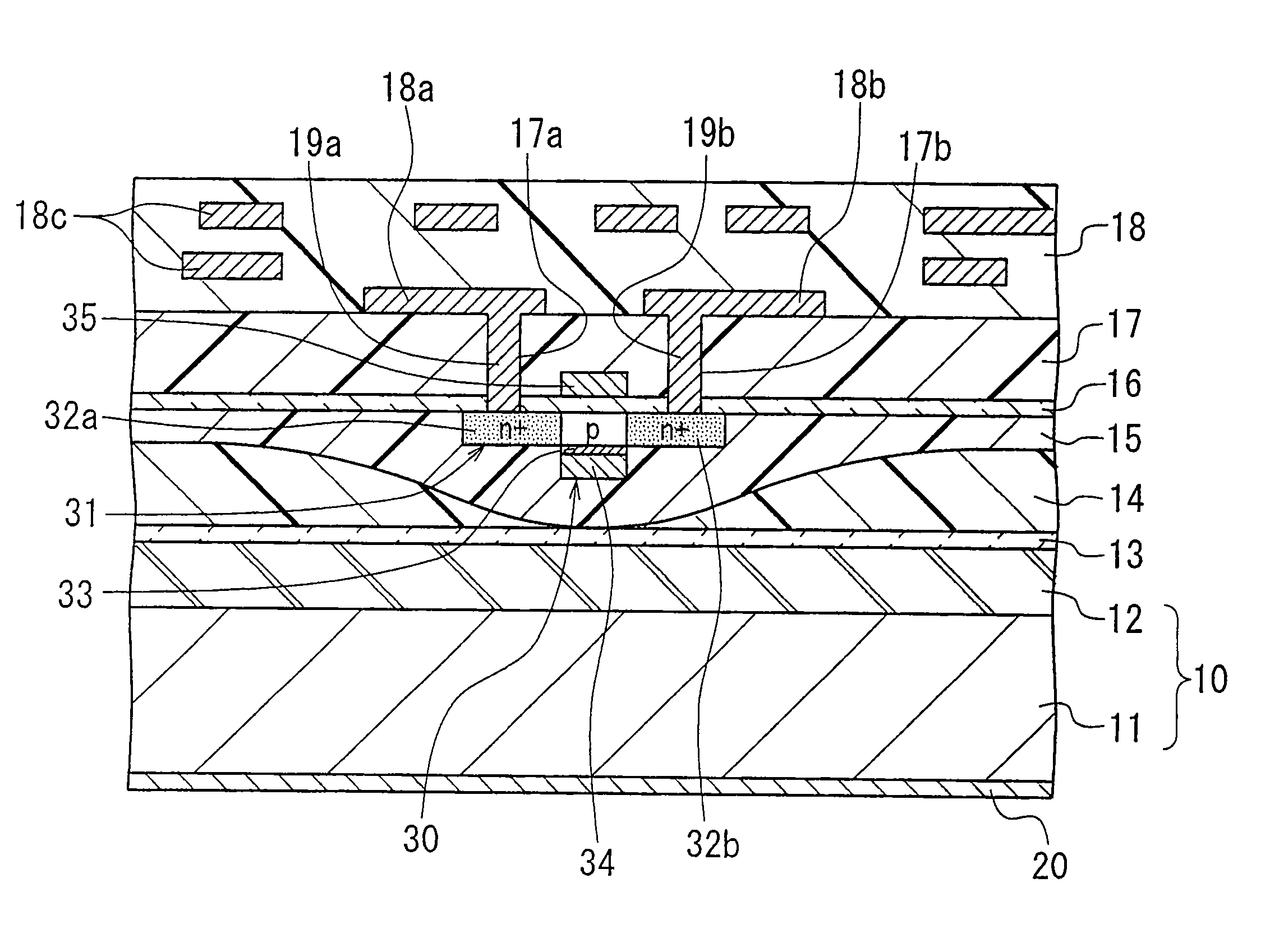
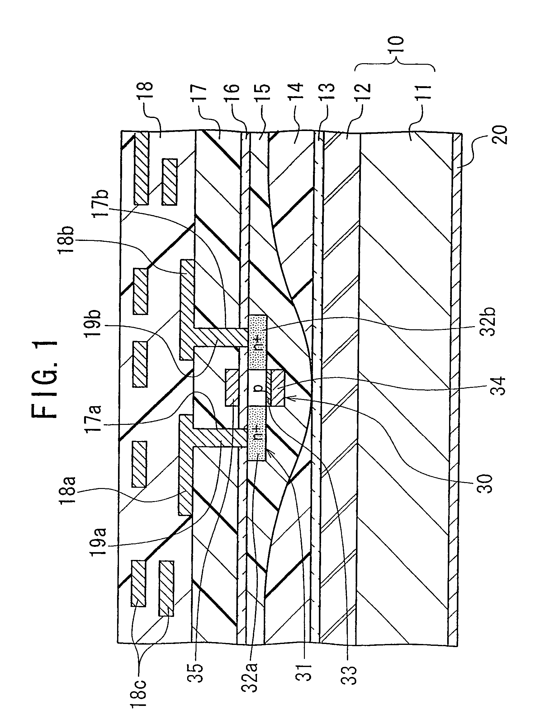
[0061]FIG. 1 is a cross-sectional view showing the configuration of a main part of a semiconductor device according to a first embodiment of the invention.
[0062] As shown in FIG. 1, the semiconductor device according to the first embodiment comprises a substrate 11, and a low dielectric constant material film 12 formed on the substrate 11. The substrate 11 and the film 12 constitute a base 10. The base 10 has such rigidity as to support the multilayer structure formed thereon. The surface of the film 12 forms the first surface of the base 10. The second surface of the base 10 is formed by the back surface of the base 11.
[0063] A semiconductor element layer including a MOS transistor 30 is fixed on the first surface of the base 10, i.e., on the surface of the low dielectric constant material film 12, with an adhesive film 13. The semiconductor element layer is constituted by the MOS transistor 30, interlayer insulator films 14 and 15, and insulator films 16 and 17. Further, a multi...
second embodiment
[0110]FIG. 9 is a cross-sectional view showing the configuration of a main part of a semiconductor device according to a second embodiment of the invention.
[0111] The semiconductor device of FIG. 9 corresponds to one obtained by adding a multilayer wiring structure 51 to the semiconductor device according to the first embodiment. Therefore, by attaching the same reference symbols as used for the device of the first embodiment to the same or corresponding elements in FIG. 9, detailed explanation about them is omitted here.
[0112] As shown in FIG. 9, the multilayer wiring structure 51 is provided between the low dielectric constant material film 12 forming the base 10, and the interlayer insulator film 14, in other words, the structure 51 is located between the base 10 and the semiconductor element layer. The source / drain region 32a of the transistor 30 in the semiconductor element layer is electrically connected to the predetermined wiring of the structure 51. The structure 51 is ad...
third embodiment
[0121]FIG. 12 is a cross-sectional view showing the configuration of a main part of a semiconductor device according to a third embodiment of the invention.
[0122] The semiconductor device of FIG. 12 corresponds to one obtained by omitting the second gate electrode 35 of the MOS transistor 30 from the semiconductor device according to the first embodiment. Thus, by attaching the same reference symbols as used for the device of the first embodiment to the same or corresponding elements in FIG. 12, detailed explanation about them is omitted here.
[0123] Since the semiconductor device according to the third embodiment of the invention has substantially the same configuration as the device according to the first embodiment and therefore, it is apparent that the same advantages as those in the first embodiment are obtained.
[0124] Additionally, with the device of the third embodiment, the transistor 30 do not have the second gate electrode 35. Thus, there is an advantage that the configu...
PUM
 Abstract
Description
Claims
Application Information


