Method for forming multilayer electrode capacitor

a multi-layer electrode and capacitor technology, applied in the field of capacitor forming, can solve the problems of many electrical defects, low capacitance, and conventional methods for forming multi-layer electrode capacitors have some drawbacks

Inactive Publication Date: 2006-06-01
PROMOS TECH INC
View PDF6 Cites 62 Cited by
  • Summary
  • Abstract
  • Description
  • Claims
  • Application Information

AI Technical Summary

Benefits of technology

[0019] Another advantage of the present invention is that the present invention is suitable for producing trench capacitors or stacked capacitors.

Problems solved by technology

However, decreasing the scale of a capacitor reduces the storage capacity thereof for electrical charges and leads to low capacitance.
However, conventional methods for forming multilayer electrode capacitors have some drawbacks.
Improper positioning of the leads causes many electrical defects, such as short circuits, electric leakage or loss of charge-storage capacity.

Method used


Image

  • Method for forming multilayer electrode capacitor
  • Method for forming multilayer electrode capacitor
  • Method for forming multilayer electrode capacitor

Examples


Embodiment Construction

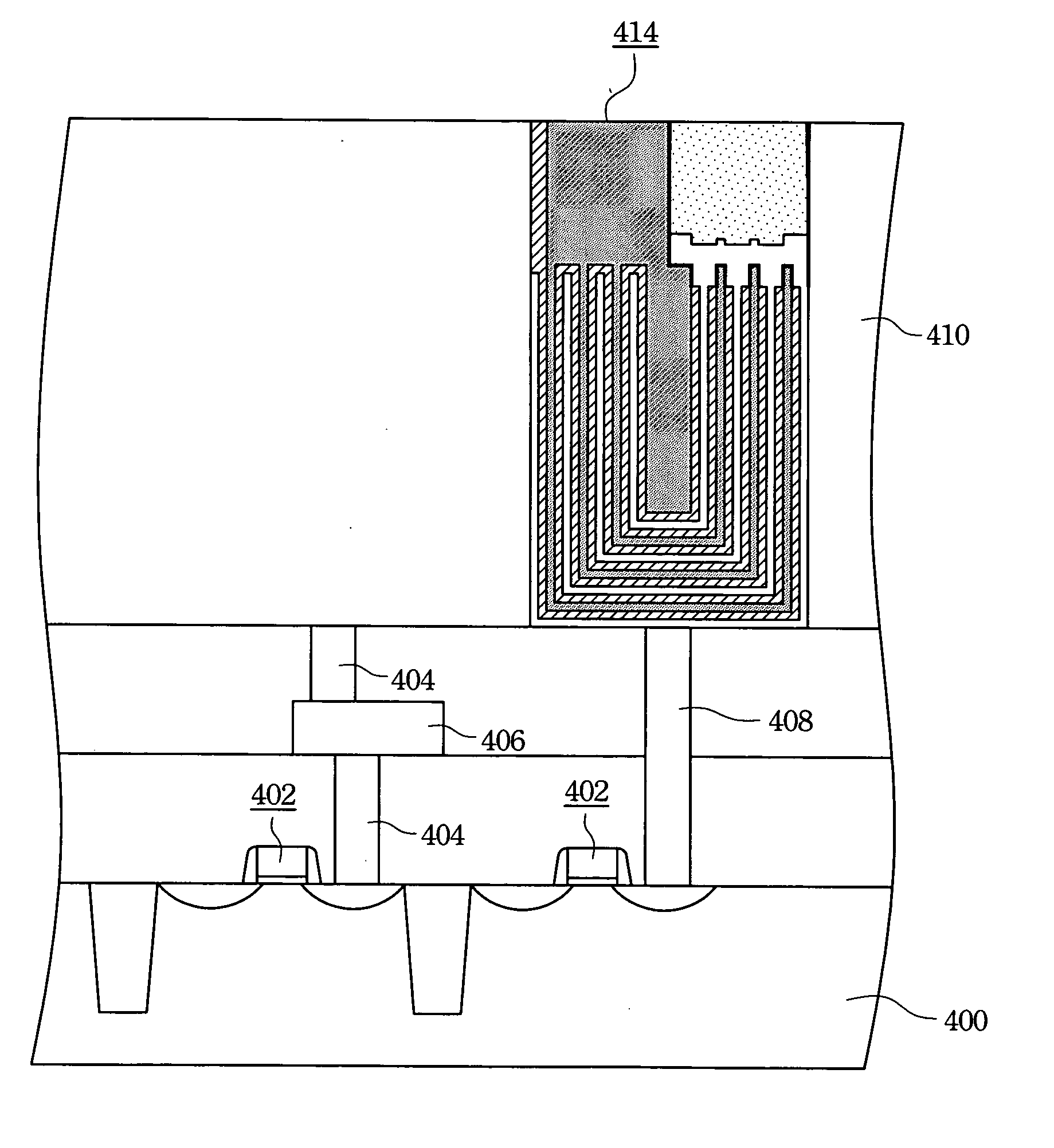
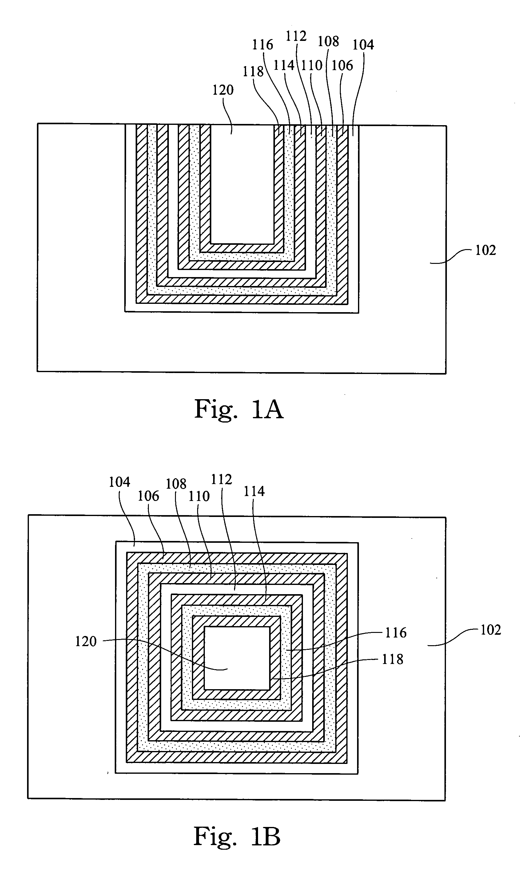
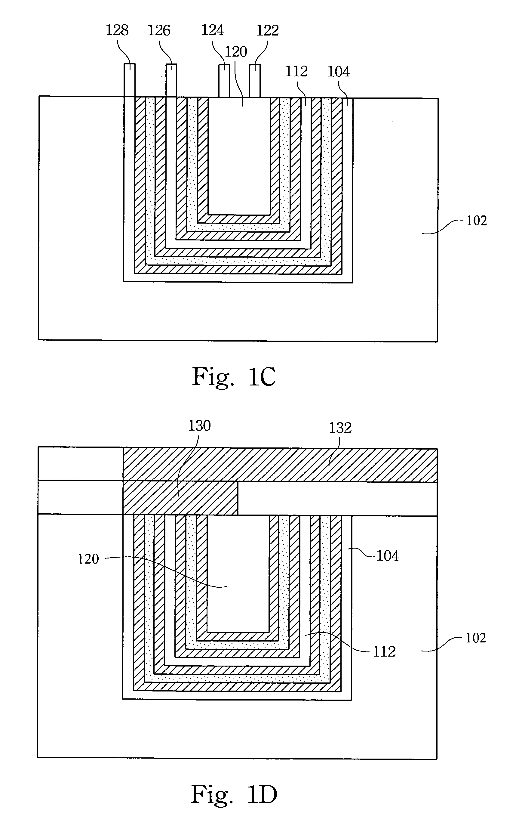
[0047] According to the present invention, methods for forming a multilayer electrode capacitor are disclosed. Referring to FIG. 2A, FIG. 2A is a flow chart showing a method for forming a multilayer electrode capacitor according to the present invention. A trench is formed in a semiconductor substrate or in the dielectric layer on the transistor of a semiconductor device by performing an etching step 200. A depositing step 202 is preformed repeatedly to deposit a first conductive layer and a second conductive layer in sequence until the trench is filled. A dielectric layer is formed between the first conductive layer and the second conductive layer. After performing a CMP and etching step 203, the respective top surfaces of the conductive layer and the dielectric layer are exposed, and a recess depth from the top of the layers to the top of the trench is formed.

[0048] The first conductive layer, the second conductive layer, and the dielectric layer are different in height by perfor...


PUM


Abstract

A method of forming a multilayer electrode capacitor is described. A trench is formed in a substrate or in an insulator layer. Two sets of conductive layers are deposited on the inner surface of the trench. The first set of conductive layers is electrically connected to each other, and so is the second set of conductive layers. Each of the second set of conductive layers is inserted between two first conductive layers, and dielectric layers are interposed between two conductive layers to form a multilayer electrode capacitor.

Description

BACKGROUND [0001] 1. Field of Invention [0002] The present invention relates methods for forming capacitors, and particularly to a method for forming a multilayer-electrode capacitor. [0003] 2. Description of Related Art [0004] In semiconductor industries, there is a trend to increase the integration and to decrease the scale of semiconductor devices. However, decreasing the scale of a capacitor reduces the storage capacity thereof for electrical charges and leads to low capacitance. Therefore, a method to form capacitors with a high capacitance value and without increasing the size thereof is desired. [0005] Capacitors can be divided into stacked capacitors and trench capacitors according to the production methods thereof. Stacked capacitors are formed on the dielectric layer on a device after finishing all features (such as transistors) and interconnecting lines. The production method for stacked capacitors is simpler and cheaper than that for trench capacitors. But because of the...

Claims


Application Information

Patent Timeline
Patent Type & Authority Applications(United States)
IPC IPC(8): H01L21/00
CPCH01L21/76895H01L27/10855H01L27/10867H01L28/91H01L29/417H01L29/66181H01L29/945H10B12/0385H10B12/0335
Inventor WU, HSIAO-CHE
Owner PROMOS TECH INC
Why Eureka
Try Eureka