Pulse-rejecting circuit for suppressing single-event transients

a single-event, pulse-rejecting technology, applied in the direction of logic circuits, pulse automatic control, pulse technique, etc., can solve the problems of solid-state circuits being vulnerable to disturbances, loading wrong data states into latches, and likely problems

Inactive Publication Date: 2006-06-08
HONEYWELL INT INC
View PDF53 Cites 27 Cited by
  • Summary
  • Abstract
  • Description
  • Claims
  • Application Information

AI Technical Summary

Benefits of technology

[0015] According to the embodiment, the pulse-rejecting circuit can be connected in a signal path between a first logic block that provides the input signal and a second logic block that receives the output signal, such that transient pulses occurring on the input signal are blocked from appearing within the output signal provided to the second logic block. In one example, the first logic block could be combinational logic, whereas the second logic block could be a memory element, such as a random access memory (RAM), latch, flip-flop, or a register. Advantageously, SETs rejected from signals provided to the memory element will not cause SET-induced upsets within that element.

Problems solved by technology

Such solid-state circuits are vulnerable to disturbances caused by single, charged particles.
If the particle strike results in a bit flip or other form of corruption of stored data, this is known as a single-event upset (SEU), or a soft error.
What is likely to be a problem is the consequence of having a temporary voltage disturbance on a circuit node.
However, if the data input does not recover to the valid state from the SET before the latch closes, then the wrong data state is loaded into the latch.
As the feature sizes continue to decrease, SETs are more likely to propagate through logic gates as normal logic pulses, causing upsets within logic circuits.

Method used


Image

  • Pulse-rejecting circuit for suppressing single-event transients
  • Pulse-rejecting circuit for suppressing single-event transients
  • Pulse-rejecting circuit for suppressing single-event transients

Examples


Embodiment Construction

1. Overview

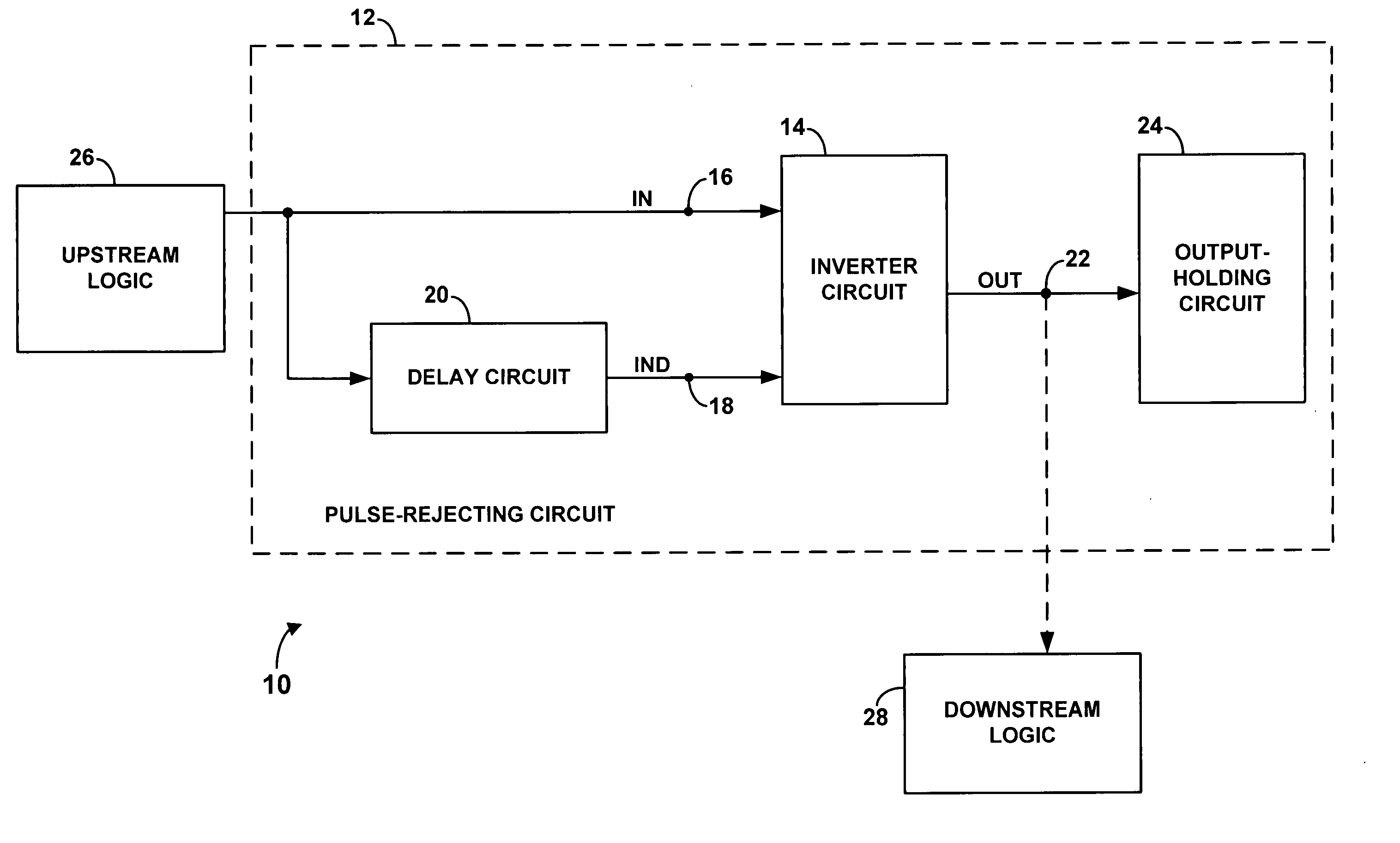
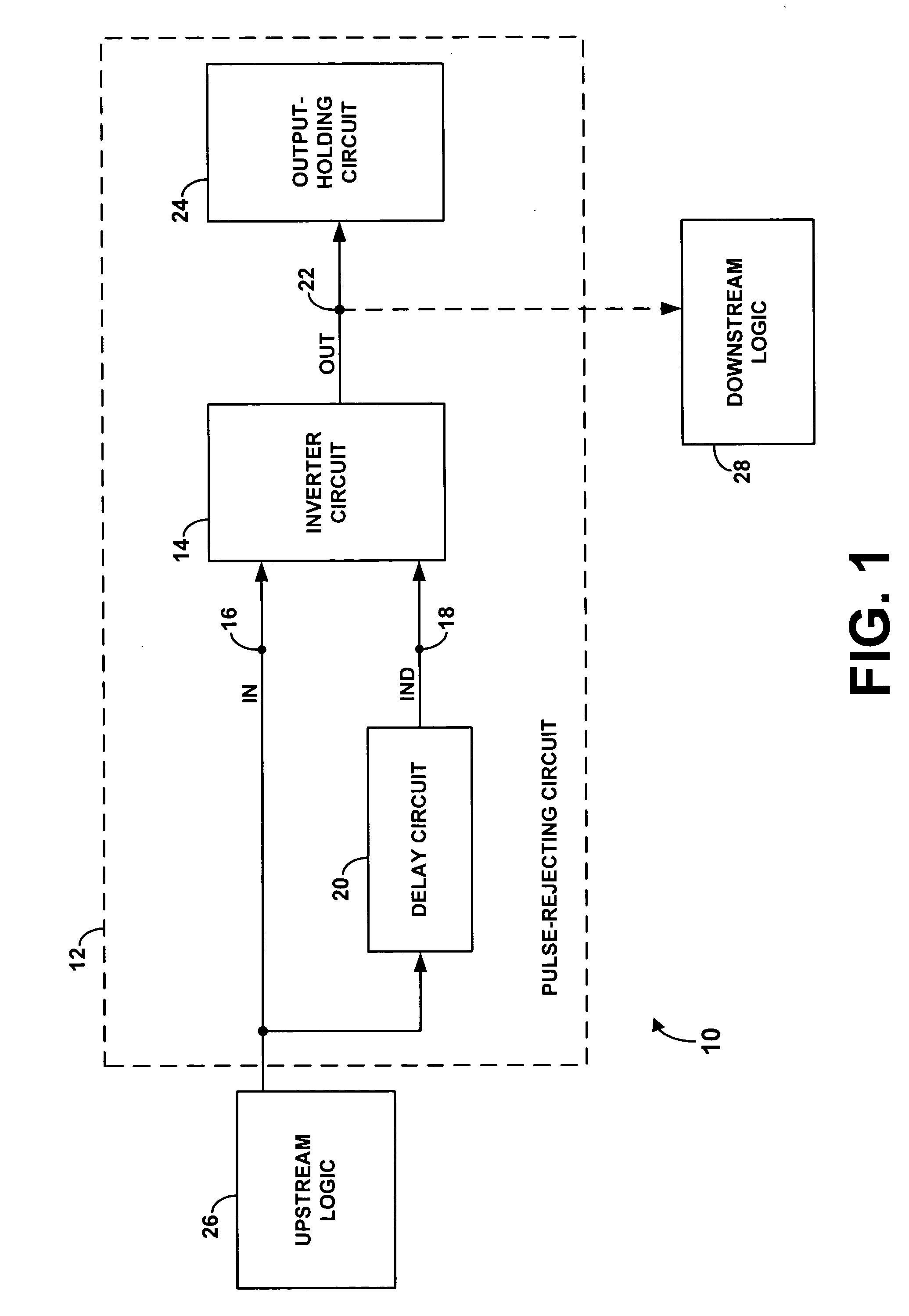
[0026]FIG. 1 illustrates a simplified block diagram of a logic circuit 10, which includes a pulse-rejecting circuit 12 in accordance with a disclosed embodiment of the present invention. As illustrated in FIG. 1, pulse-rejecting circuit 12 comprises an inverter circuit 14 that receives input signals via a direct input 16 and a delayed input 18, a delay circuit 20 coupled to delayed input 18, and an output-holding circuit 24 coupled to an output 22 of inverter circuit 14. Additionally, direct input 16 may be coupled to an upstream logic block 26, whereas output 22 may coupled to a downstream logic block 28.

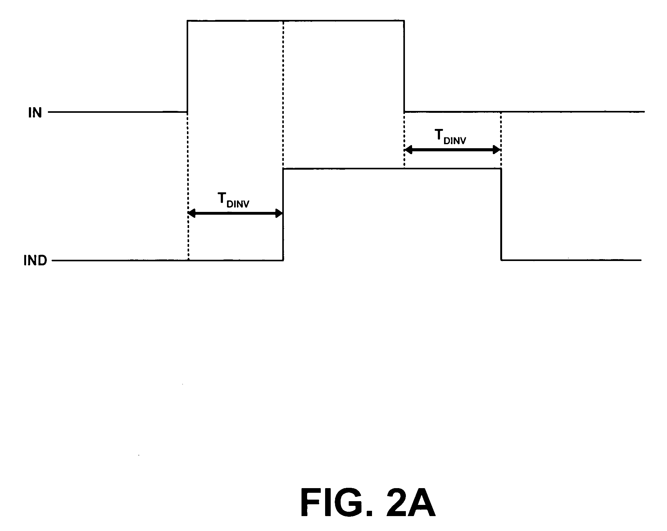
[0027] In operation, an input signal IN and a time-delayed version of the IN signal are fed into inverter circuit 14 via respective direct input 16 and delayed input 18. More particularly, as shown in FIG. 1, the IN signal present on direct input 16 passes through delay circuit 20 and appears on delayed input 18 as a time-delayed input signal IND. For the purposes of ...


PUM


Abstract

A circuit for rejecting single-event transients (SETs) from logic signals is provided. The circuit includes a delay circuit, an inverter circuit, and an output-holding circuit. The delay circuit receives an input signal and delays the input signal to produce a time-delayed version of the input signal. The input signal and the time-delayed version of the input signal are fed into the inverter circuit that propagates a corresponding output signal only when the input signal and the time-delayed version of the input signal have the same logic level. If the input signal or the time-delayed version of the input signal transitions such that both input signals presented to the inverter circuit have opposite logic levels, the output-holding circuit maintains the output signal in its previous state.

Description

GOVERNMENT RIGHTS [0001] The United States Government has acquired certain rights in this invention pursuant to Contract No. DTRA01-02-D-0008 awarded by the Defense Threat Reduction Agency (DTRA).BACKGROUND [0002] 1. Field of the Invention [0003] The present invention generally relates to particle-induced disturbances in microelectronic circuits and, more particularly, to suppressing transient pulses occurring within logic signals. [0004] 2. Description of Related Art [0005] Integrated circuits used in space, weapons, or aviation applications must be more resistant to radiation than circuits used in other applications, because they are more likely to be exposed to radiation, and because their reliability is often more critical. Such solid-state circuits are vulnerable to disturbances caused by single, charged particles. Some examples of these particles are: [0006] Alpha particles: These are the byproducts of the natural decay of elements such as uranium and thorium present in some i...

Claims


Application Information

Patent Timeline
Patent Type & Authority Applications(United States)
IPC IPC(8): H03K5/08
CPCH03K19/00338
Inventor CARLSON, ROY M.
Owner HONEYWELL INT INC
Why Eureka
Try Eureka