Method for solder bumping, and solder-bumping structures produced thereby

a technology of solder bumping and solder bumping, which is applied in the direction of resist details, printed circuit manufacturing, patterning and lithography, etc., can solve the problems of excessive total package cost, ever-increasing demands, and long time-consuming for skilled in the art to find the solution

Active Publication Date: 2006-06-15
JCET SEMICON (SHAOXING) CO LTD
View PDF6 Cites 23 Cited by
  • Summary
  • Abstract
  • Description
  • Claims
  • Application Information

AI Technical Summary

Problems solved by technology

Electronic packaging techniques, for example systems-in-package (“SiP”) that use such wafer level CSP formats, thus face ever-increasing demands.
But due to high equipment costs and high solder sphere costs, available techniques result in excessive total package costs.
Solutions to these problems have been long sought but prior developments have not taught or suggested any solutions and, thus, solutions to these problems have long eluded those skilled in the art.

Method used


Image

  • Method for solder bumping, and solder-bumping structures produced thereby
  • Method for solder bumping, and solder-bumping structures produced thereby
  • Method for solder bumping, and solder-bumping structures produced thereby

Examples


Embodiment Construction

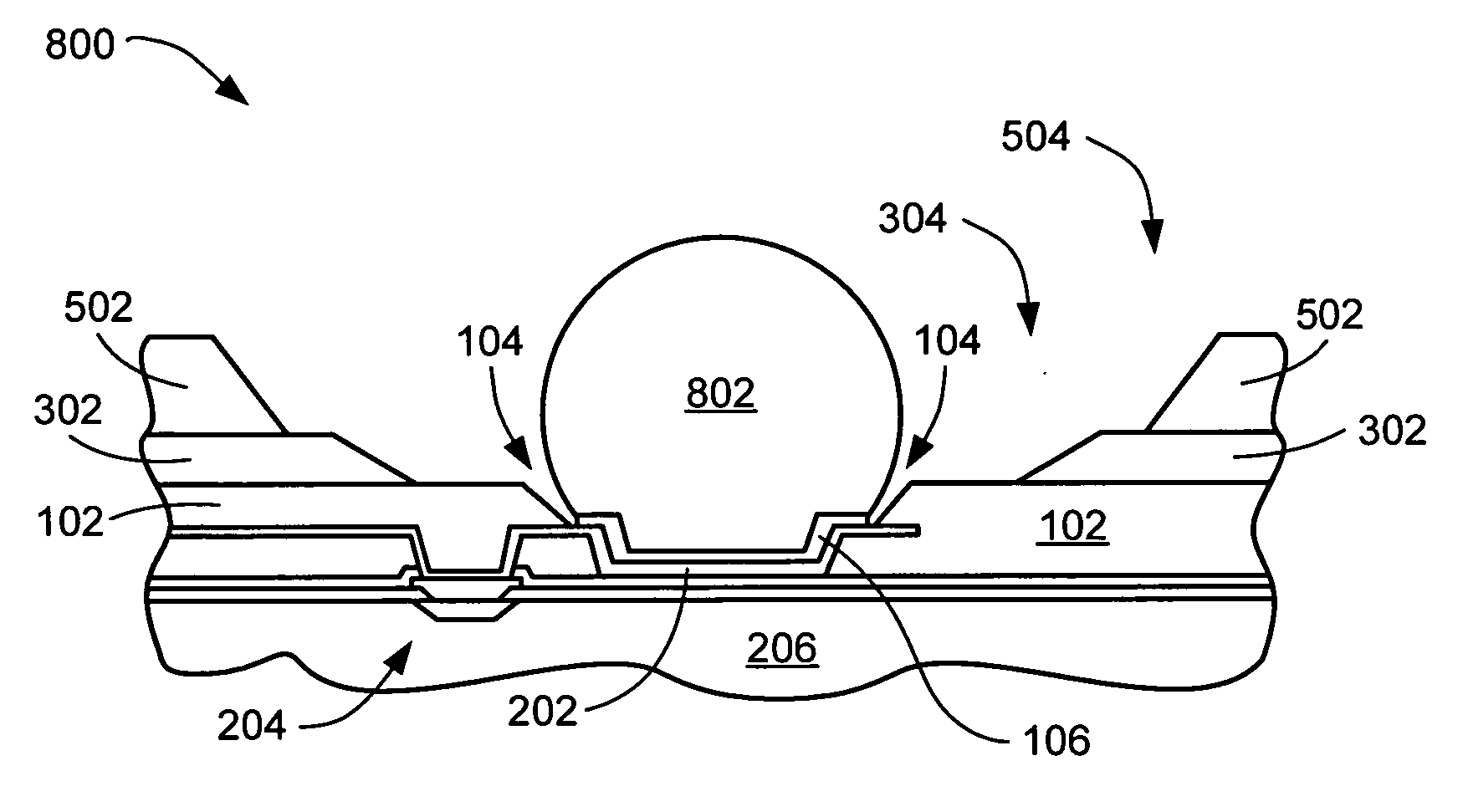
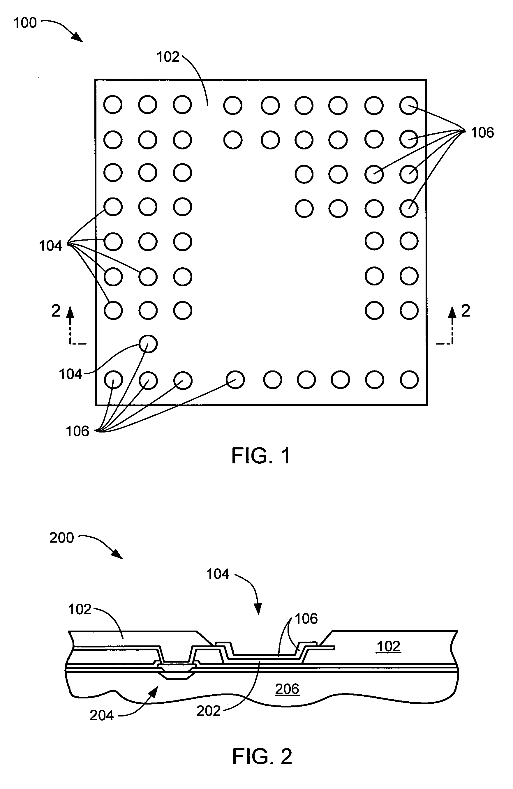
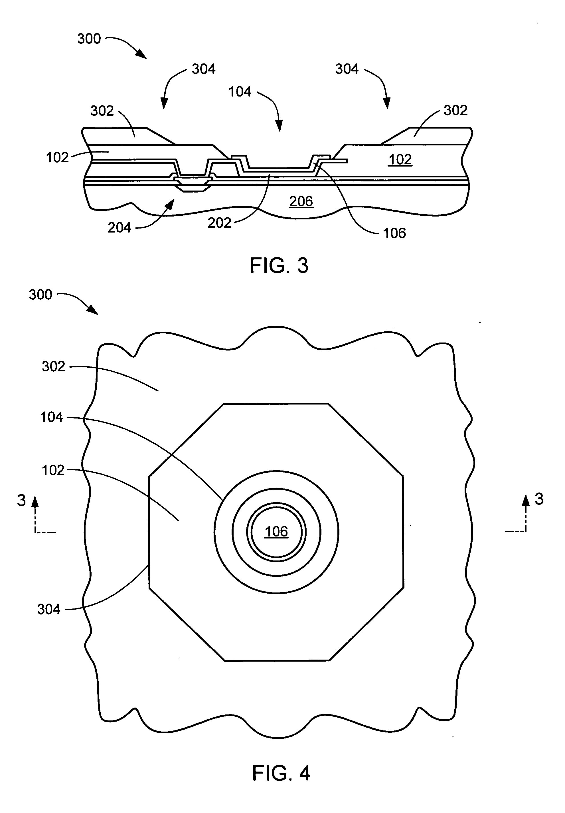
[0026] In the following description, numerous specific details are given to provide a thorough understanding of the invention. However, it will be apparent that the invention may be practiced without these specific details. In order to avoid obscuring the present invention, some well-known configurations and process steps are not disclosed in detail.

[0027] Similarly, the drawings showing embodiments of the invention are semi-diagrammatic and not to scale and, particularly, some of the dimensions are for the clarity of presentation and are shown exaggerated in the FIGs. Additionally, where multiple embodiments are disclosed and described having some features in common, for clarity and ease of illustration, description, and comprehension thereof, similar and like features one to another will ordinarily be described with like reference numerals.

[0028] The term “horizontal” as used herein is defined as a plane parallel to the conventional plane or surface of the chip or wafer, regardl...


PUM

PropertyMeasurementUnit
thicknessaaaaaaaaaa
thicknessaaaaaaaaaa
equivalent diameteraaaaaaaaaa

Abstract

A method for solder bumping provides a substrate and forms a film on the substrate. The film has openings therethrough. A stencil is aligned on the film. The stencil has openings therethrough over the openings through the film. Solder paste is printed onto the substrate and into the openings through the stencil and the openings through the film. The solder paste is reflowed to form solder balls therefrom. The stencil and the film are then removed.

Description

TECHNICAL FIELD [0001] This invention relates to packaged semiconductor devices and methods for the manufacture thereof. More particularly, the invention pertains to solder bumping methods for producing large solder bumps for such devices, and to semiconductor devices that are provided with such large solder bumps. BACKGROUND ART [0002] Solid-state electronic devices (e.g., semiconductor “chips” or “dies”) are typically manufactured from a semiconductor material such as silicon, germanium arsenide, or gallium arsenide. Circuitry is formed on one surface, and includes input and output (“I / O”) pads to facilitate electrical connection to other circuit components. [0003] Semiconductor chips are usually packaged for protection from mechanical damage, external contamination, and moisture. Typically, packages encapsulate the semiconductor chips within a polymeric or ceramic material. [0004] As the configurations of electronic products become more and more light and compact, semiconductor c...

Claims


Application Information

Patent Timeline
Patent Type & Authority Applications(United States)
IPC IPC(8): H01L23/48H01L21/60
CPCH01L24/11H01L2224/0401H01L2224/13099H01L2224/13111H01L2224/16H01L2924/01027H01L2924/01029H01L2924/01032H01L2924/01078H01L2924/01079H01L2924/01082H01L2924/14H01L2924/30105H01L2924/30107H05K3/1216H05K3/3452H05K3/3484H05K2203/043H05K2203/0568H01L2224/05027H01L24/13H01L2224/05018H01L2224/05558H01L2224/13021H01L2924/01006H01L2924/01024H01L2924/01033H01L2924/014H01L2224/05572H01L2924/0002H01L2224/1132H01L2224/05552H01L24/05H01L2224/0236H01L2224/05008H01L2224/05147H01L2224/05171H01L2224/05555H01L2224/05569H01L2224/05644H01L2224/05647H01L2224/0616H01L2224/11849H01L2924/15787H05K3/3485H01L2924/00H01L2924/00014H01L2924/00012H01L2924/013
Inventor DO, BYUNG TAIALVAREZ, ROMEO EMMANUEL P.LIN, YAOJIAN
Owner JCET SEMICON (SHAOXING) CO LTD
Why Eureka
Try Eureka