
Optical device and drive voltage supply device

Inactive Publication Date: 2006-06-15
FUJITSU LTD
View PDF5 Cites 2 Cited by
  • Summary
  • Abstract
  • Description
  • Claims
  • Application Information

AI Technical Summary

Benefits of technology

[0019] The present invention has been conceived in view of such a problem and prevents occurrence of a d.c. drift and enables selection of stable light of desired wavelength without deteriorating a filtering characteristic.
[0025] According to the present invention, a voltage value applied to individual comb-shaped electrode pairs is changed with time, and hence unbalanced concentration of ions in the buffer layer can be averaged with time, thereby preventing occurrence of a d.c. drift. Therefore, there can be realized an optical device which entails few fluctuations in an effective voltage applied to the individual comb-shaped electrode pairs and which enables selection of a stable wavelength.

Problems solved by technology

However, as mentioned previously, when the d.c. voltage is fixedly applied to the respective comb-shaped electrode pairs 805, an unbalanced concentration of ions arises in the buffer layer 1201 for reasons of a constant electric field stemming from application of the d.c. voltage.
This induces a change in the value of the applied voltage set in advance for the comb-shaped electrode pair 805 (this phenomenon is called a d.c. drift), which in turn yields a problem of a failure to achieve a desired filtering characteristic.

Method used


Image

  • Optical device and drive voltage supply device
  • Optical device and drive voltage supply device
  • Optical device and drive voltage supply device

Examples


Embodiment Construction

[A] Description of an Embodiment

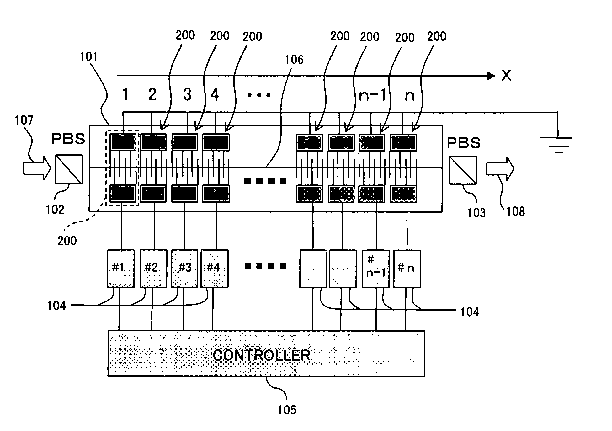
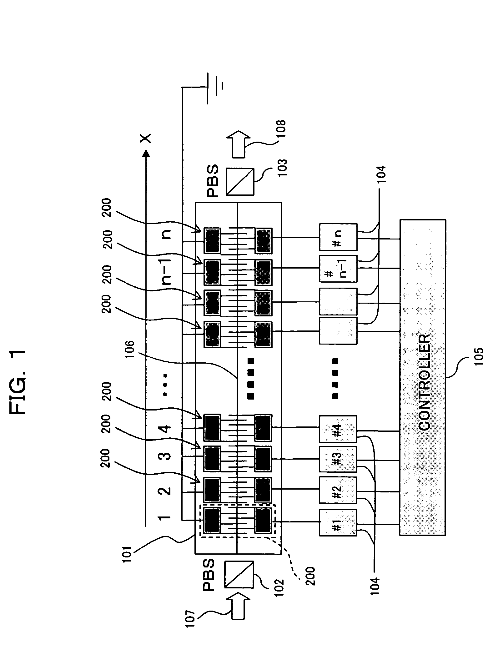
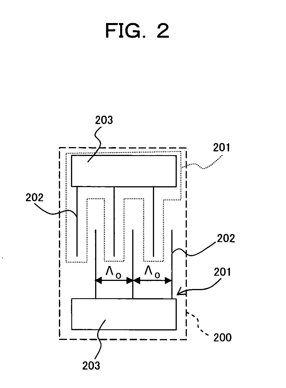
[0038]FIG. 1 is a block diagram showing the configuration of an EOTF serving as an optical device according to an embodiment of the present invention and the configuration of a drive circuit (a drive voltage supply device) of the EOTF. As shown in FIG. 1, this EOTF also comprises a substrate 101; a preceding-stage polarized beam splitter (PBS) 102; and a subsequent-stage polarized beam splitter (PBS) 103. The drive circuit comprises a plurality (#1 to #n: “n” is an integer equal to 2 or more) of a.c. power sources 104, and a controller 105. The substrate 101 comprises an optical waveguide 106, and a plurality (#1 to #n) of comb-shaped electrode pairs 200 arranged along the direction of the optical waveguide 106 (the direction of an X axis). Even in the embodiment, as mentioned previously by reference to FIG. 12, a comb-shaped electrode part 202 (which will be described later by reference to FIG. 2) of a comb-shaped electrode pair 200 crossing the opt...


PUM


Abstract

The present invention is directed toward an optical device and a drive voltage supply device, which prevent occurrence of a d.c. drift and enable stable selection of light of desired wavelength without deteriorating a filtering characteristic. The optical device comprises a substrate having an electrooptical effect; an optical waveguide formed in this substrate; a plurality of comb electrode pairs which are arranged side by side along the optical waveguide, can apply an electric field for said electrooptical effect, and are formed from respective pairs of comb electrodes; and drive voltage supply means capable of supplying a drive voltage to said comb electrode pairs such that the voltage changes with time.

Description

1) FIELD OF THE INVENTION [0001] The present invention relates to an optical device and a drive voltage supply device; for instance, a technique suitable for use in a wavelength filter such as an electro-optic tunable filter (EOTF: Electro-Optic Tunable Filter) or the like. 2) DESCRIPTION OF THE RELATED ART [0002] Recent development of optical communication techniques has enabled high-capacity, high-speed communication. One of the techniques that embody high-capacity, high-speed communication is wavelength division multiplexing (WDM). This technique is for simultaneously using a plurality of optical signals of different wavelengths and efficiently utilizing a transmission band of a transmission path. [0003] In relation to a WDM communications system, there is sought a function for multiplexing / demultiplexing a plurality of wavelengths or switching a path on a per-wavelength basis between fibers which serve as transmission paths of optical signals. A fixed filter and a variable wavel...

Claims


Application Information

Patent Timeline
IPC IPC(8): G02F1/035
CPCG02F1/0353G02F2201/124
Inventor NAKAZAWA, TADAONAKAZAWA, YUMIMIYATA, HIROSHITSUNODA, YUKITO
Owner FUJITSU LTD
Features
  • Generate Ideas
  • Intellectual Property
  • Life Sciences
  • Materials
  • Tech Scout
  • Unparalleled Data Quality
  • Higher Quality Content
  • 60% Fewer Hallucinations
Learn More