Image display apparatus and driving method thereof

a technology of image display and driving method, which is applied in the direction of instruments, television systems, ventilation systems, etc., can solve the problems of increasing the significance of problems, the difference in brightness per predetermined number of pixels driven by the common electrode cannot be fully eliminated, and the impedance and sustain current cannot be completely eliminated. , to achieve the effect of improving the quality of display imag

Inactive Publication Date: 2006-06-22
MAXELL HLDG LTD
View PDF8 Cites 19 Cited by
  • Summary
  • Abstract
  • Description
  • Claims
  • Application Information

AI Technical Summary

Benefits of technology

[0023] According to the present invention, without increasing the large-sized circuits and the manufacture costs, the image display apparatus driven by the common driving voltage per predetermined number of pixels or per predetermined display region on the

Problems solved by technology

However, even through the bus impedance and the sustain current are decreased, these bus impedance and sustain current cannot completely be eliminated.
Therefore, the difference in brightness per predetermined number of pixels driven by the common electrode cannot be sufficiently resolved.
This problem has become increasingly significant with demands in recent years for larger display pane

Method used


Image

  • Image display apparatus and driving method thereof
  • Image display apparatus and driving method thereof
  • Image display apparatus and driving method thereof

Examples


embodiment

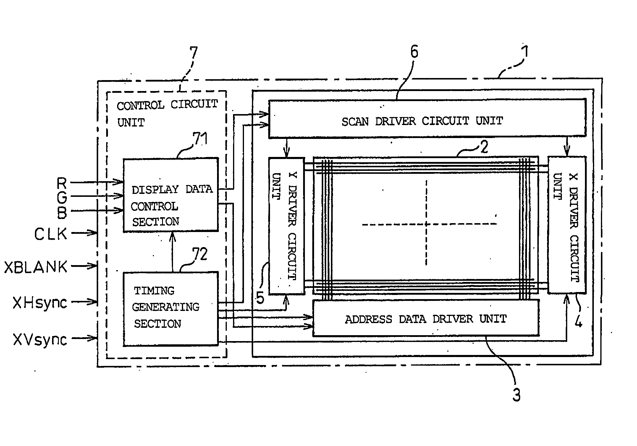
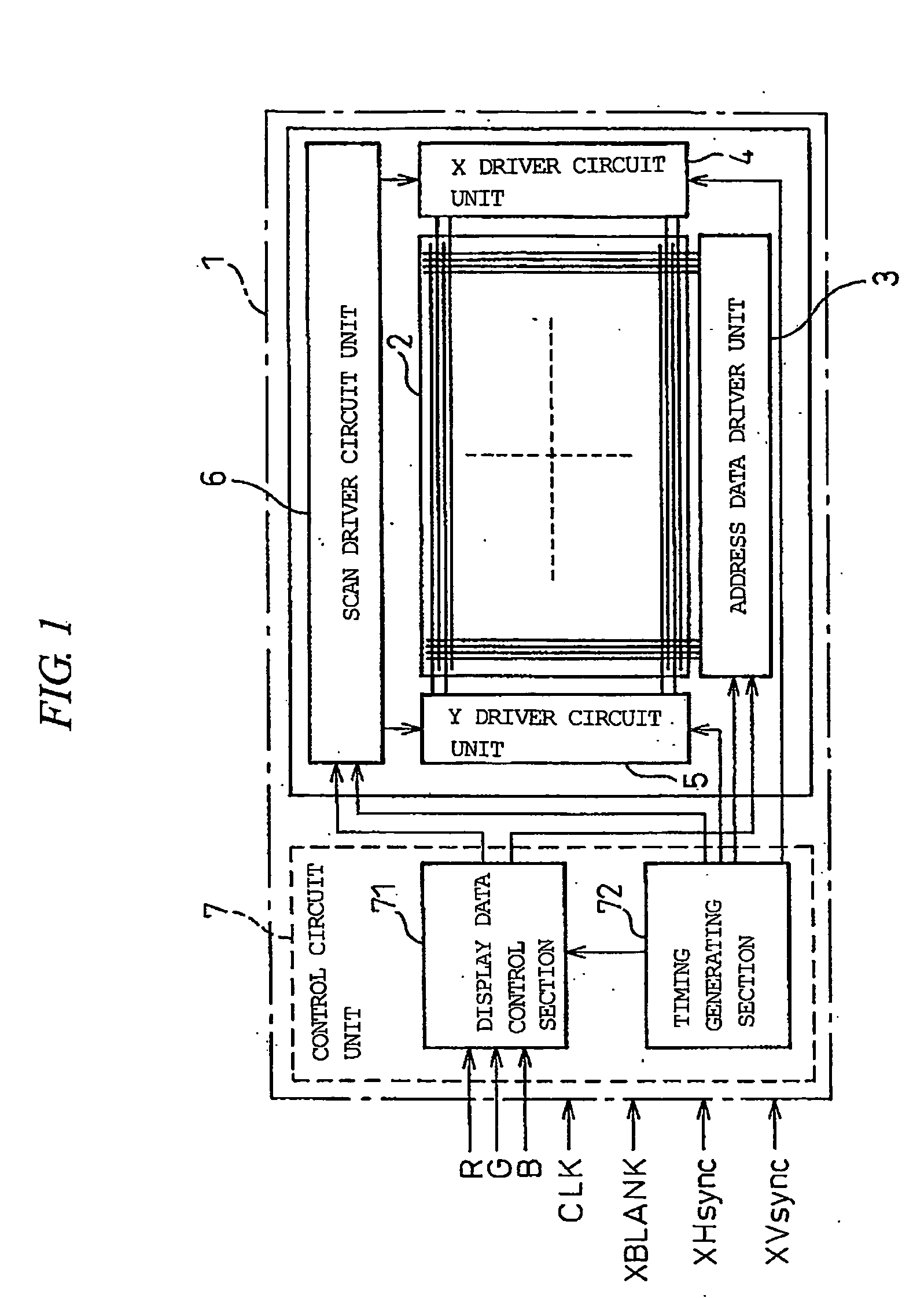
[0049]FIG. 3 is a block diagram schematically showing a plasma display apparatus as an image display apparatus according to one embodiment of the present invention, and shows one example of a three-electrode surface discharge AC plasma display apparatus. In FIG. 3, a reference numeral “10” denotes an image display apparatus, “2” denotes a display panel (PDP), “3” denotes an address data driver circuit unit, “4” denotes an X driver circuit unit, “5” denotes a Y driver circuit unit, “6” denotes a scan driver circuit unit, “7” denotes a control circuit unit, and “8” denotes a correction processing circuit unit.

[0050] As evident from a comparison between FIG. 3 and FIG. 1 described above, in summary, the image display apparatus (plasma display apparatus) 10 according to the present embodiment is equivalent to the conventional plasma display apparatus 1 having added thereto the correction processing circuit unit 8.

[0051] That is, the plasma display apparatus 10 according to the present...


PUM


Abstract

In a conventional image display apparatus, since display load ratios for respective lines are different, voltage drop amounts are also different and a difference in brightness occurs in spite of giving the same inputted luminance signal, so that image quality of display image is degraded. In the case where signals at the same luminance level are inputted and displayed, for a pixel on a display panel, an ON pattern of a subfield in one field is changed when a line load ratio of a line including the pixel is changed. That is, an image display apparatus using a display panel having a plurality of pixels is configured so as to include, for each of the plurality of pixels connected to one driving electrode, a load calculating means that calculates the load ratio and a luminance correcting means that calculates a drop amount in luminance level of an inputted video signal for correction.

Description

CROSS-REFERENCE TO RELATED APPLICATION [0001] The present application claims priority from Japanese patent application No. JP 2004-351569 filed on Dec. 3, 2004 and No. JP 2005-101325 filed on Mar. 31, 2005, the contents of which are hereby incorporated by reference into this application. BACKGROUND OF THE INVENTION [0002] The present invention relates to an image display apparatus and its driving method and, particularly, to the image display apparatus driven by a common driving electrode per predetermined number of pixels or per predetermined display region on a display panel and to the driving method thereof. [0003] Conventionally, a plasma display apparatus using a plasma display panel (PDP) for a surface discharge has been commercially available as a flat-type image display apparatus, and has been used as, for example, a display apparatus such as a personal computer and a work station, a flat-type wall-mounted television, and a apparatus for displaying advertisements, informatio...

Claims


Application Information

Patent Timeline
IPC IPC(8): H04N5/21H04N9/78H04N9/77G09G3/288G09G3/20G09G3/28G09G3/291G09G3/293G09G3/298G09G3/36
CPCG09G3/20G09G3/2003G09G3/2022G09G3/298G09G3/30G09G2320/0223G09G2320/0233G09G2320/0626G09G2320/0666G09G2320/0673G09G2330/021G09G2360/16F24F7/02F24F2013/1433F24F2013/1466
Inventor KIMURA, YUICHIROOHTA, SHUNJIMIYAZAKI, YOSHINORI
Owner MAXELL HLDG LTD
Why Eureka
Try Eureka