

Level shift circuit and method
a level shift circuit and level shift technology, applied in logic circuits, pulse techniques, digital storage, etc., can solve the problems of increasing delay time, degrading responsiveness, and inability to detect the voltage level rise of bit lines, so as to increase the delay time effect of degrading responsiveness
- Summary
- Abstract
- Description
- Claims
- Application Information
AI Technical Summary
Benefits of technology
Problems solved by technology
Method used
Image

Examples
first embodiment
[0051]FIG. 4 is a detailed circuit diagram of a level shift circuit for generating a signal for delaying a rising edge of an input signal according to FIG. 3.
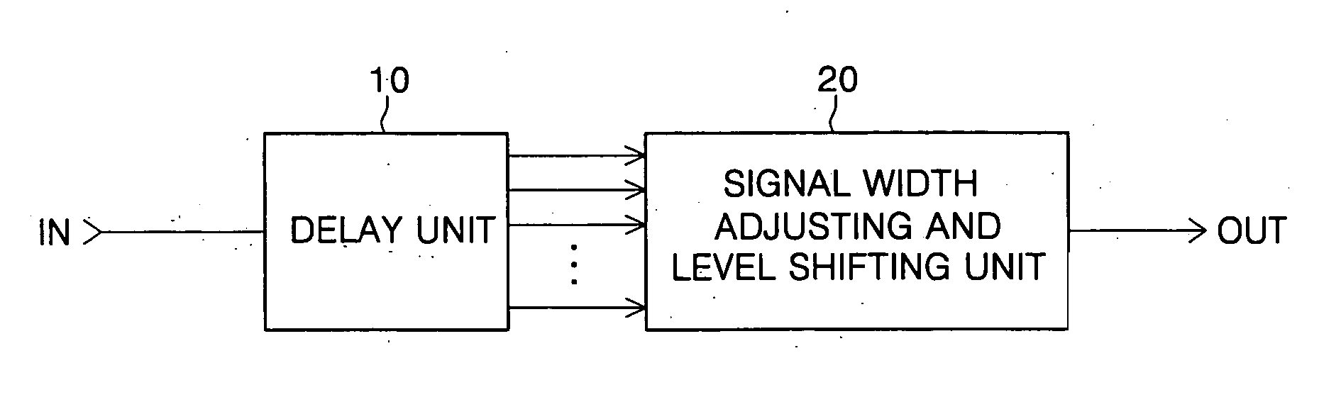
[0052] As shown in FIG. 4, a delay unit 110 delays an input signal IN with, e.g., an even number of stages to generate an even number of delayed signals. A signal width adjusting and level shifting unit 120 generates a signal transitioned from a low level to a high level in response to the input signal IN and a delayed signal from the last stage INV14 having the same phase as that of the input signal IN. And the unit 120 generates a signal transitioned from a high level to a low level in response to a delayed signal from an odd stage INV11 having a different phase from that of the input signal IN.
[0053] The delay unit 110 includes an even number of serially-connected inverters INV11 to INV14. The signal width adjusting and level shifting unit 120 includes first and second NMOS transistors NMOS11 and NMOS12 connected in series ...
third embodiment
[0083]FIG. 8 is a detailed circuit diagram of a level shift circuit for delaying a falling edge of an input signal according to FIG. 3.
[0084] As shown in FIG. 8, a delay unit 310 delays an input signal IN via an odd number of stages to generate an odd number of delayed signals. A signal width adjusting and level shifting unit 320 generates a signal transitioned from a low level to a high level in response to the input signal IN and, a signal transitioned from a high level to a low level in response to delayed signals from at least two odd stages INV31 and INV35 having a different phase from that of the input signal IN.
[0085] The delay unit 310 includes an odd number of inverters INV31 to INV35. The signal width adjusting and level shifting unit 320 includes a first NMOS transistor NMOS31 connected in series between a control node NA and a ground voltage VSS and responding to the input signal IN. The second and third NMOS transistors NMOS32 and NMOS33 are connected in series between...
fifth embodiment
[0110]FIG. 12 is a detailed circuit diagram of a level shift circuit for generating a signal enabled in synchronization with a rising edge of an input signal according to FIG. 3.
[0111] As shown in FIG. 12, a delay unit 510 delays an input signal IN via an odd number of stages to generate an odd number of delayed signals. A signal width adjusting and level shifting unit 520 generates a signal transitioned from a low level to a high level in response to the input signal IN and a delayed signal from an odd stage INV55 having a different phase from that of the input signal IN, and a signal transitioned from a high level to a low level in response to a delayed signal from an odd stage INV51 having a different phase from that of the input signal IN and a delayed signal from an even stage INV54 having the same phase as that of the input signal IN.
[0112] The delay unit 510 includes an odd number of serially-connected inverters INV51 to INV55. The signal width adjusting and level shifting u...
PUM
 Abstract
Description
Claims
Application Information