Stacked electronic component and manufacturing method thereof

a technology of electronic components and manufacturing methods, applied in the direction of basic electric elements, semiconductor devices, electrical equipment, etc., can solve the problems of easy peeling between stacked semiconductor elements, affecting the thickness of the package (semiconductor devices), and limiting the application of semiconductor elements, so as to reduce peeling failure and increase manufacturing costs.

Inactive Publication Date: 2006-06-29
KIOXIA CORP
View PDF83 Cites 96 Cited by
  • Summary
  • Abstract
  • Description
  • Claims
  • Application Information

AI Technical Summary

Benefits of technology

[0013] Consequently, an object of the present invention is to provide a stacked-type electronic component capable for preventing occurrences of an insulation failure, a short circuiting, and so on, caused by a contact of a bonding wire of the electronic component at the lower side with the electronic component at the upper side, and in addition, suppressing a peeling failure between the electronic components, ...

Problems solved by technology

However, in such a structure, the applicable semiconductor element is largely restricted.
However, a usage of such a thick spacer disturbs to make a package (semiconductor device) thinner.
However, there is an objection that a peeling off is easy to occur between the stacked semiconductor elements caused by, for example, a difference of thermal expansion coefficient between the insulating layer composed of a polyimide resin and the adhesive layer composed of an epoxy resin.
Such the deflection may be a cause of occurrences of a crack, and soon, of the semiconductor element, and a cause for a connection failure of the bonding wire.
Besides, a reliability at a wire connection portion may be deteriorated by diffusing an ultrasonic output at the bonding time, into the hollow portion below the protruding portion.
According to this structure, the resin sealing portion is existing under the semiconductor element at the upper side, and therefore, a bonding failure, the crack of the semiconductor element, and so on, can be prevented, but on the other hand, it is required to perform a resin sealing process after mounting the respective semiconductor elements, an...

Method used


Image

  • Stacked electronic component and manufacturing method thereof
  • Stacked electronic component and manufacturing method thereof
  • Stacked electronic component and manufacturing method thereof

Examples


first embodiment

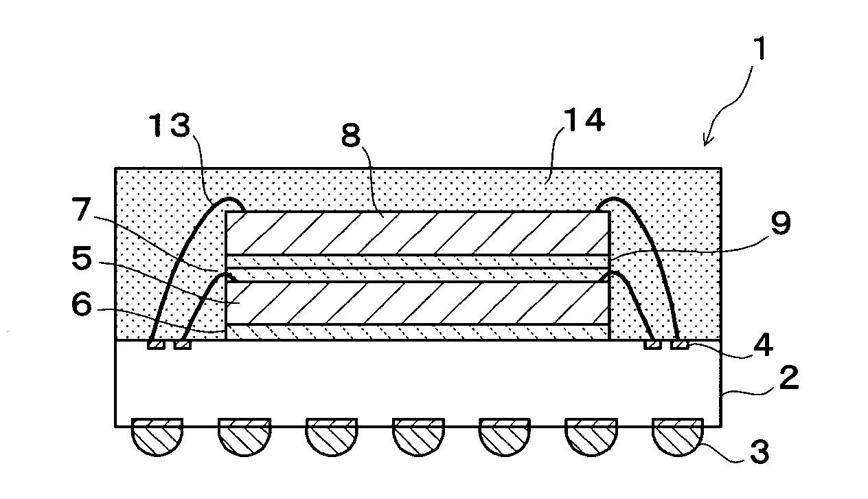
[0050]FIG. 1 is a sectional view schematically showing a configuration of a semiconductor device with a stacked-type multi chip structure (stacked-type semiconductor device) applying a stacked-type electronic component of the present invention. A semiconductor device 1 shown in the view has a substrate 2 for mounting elements. The substrate 2 is capable for mounting electronic components such as semiconductor elements, and has a circuit being electrically connected to electrodes of the semiconductor element, and so on. As such substrate 2, a circuit board in which a circuit (wiring) is formed on a surface or inside of an insulating substrate, a semiconductor substrate, and so on, or a substrate in which an element mounting portion and a circuit portion are integrated, such as a lead frame, and so on, can be used.

[0051] The semiconductor device 1 shown in FIG. 1 has a circuit board 2 as the element mounting substrate. As the insulating substrate constituting the circuit board 2, the ...

second embodiment

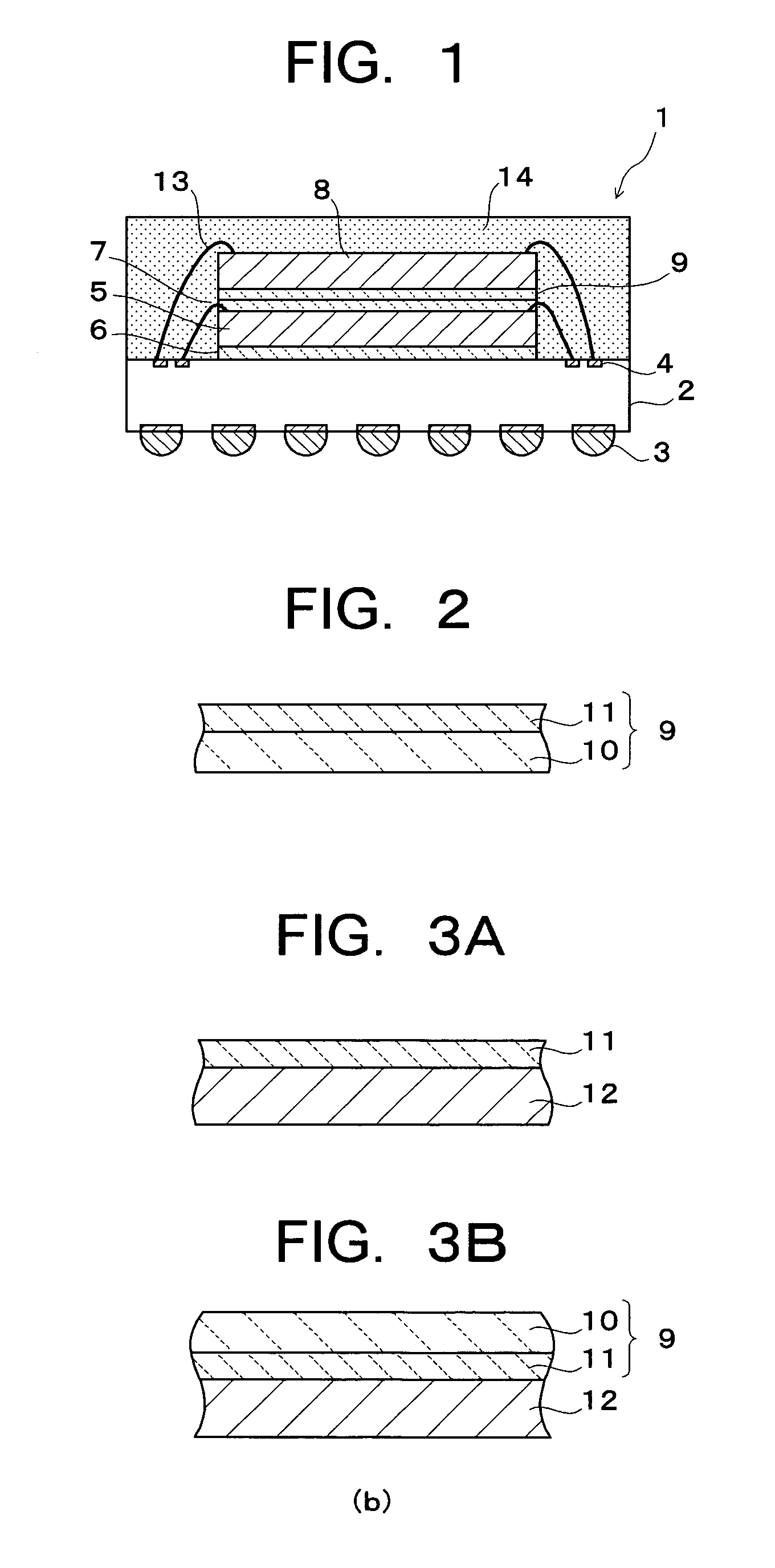
[0099] Further, the second semiconductor element 8 is offset and disposed relative to the first semiconductor element 5. Consequently, both end portions of the second semiconductor element 8 corresponding to wire bonding portions are protruding outside from an outer periphery of the first semiconductor element 5. Below these protruding portions 63, the second adhesive layer 61 is filled by softened or melted at a heating temperature (adhesive temperature) when the second semiconductor element 8 is adhered. Namely, a part of the second adhesive layer 61 softened or melted at the heating temperature is filled below the protruding portions 63 of the second semiconductor element 8, so that hollow portions below the protruding portions 63 do not appear. A thickness of the second adhesive layer 61 is preferable to be set accordingly in consideration with a filling amount of the hollow portions, as same as the

[0100] According to the above-stated semiconductor device 60 of the fourth embodi...

fifth embodiment

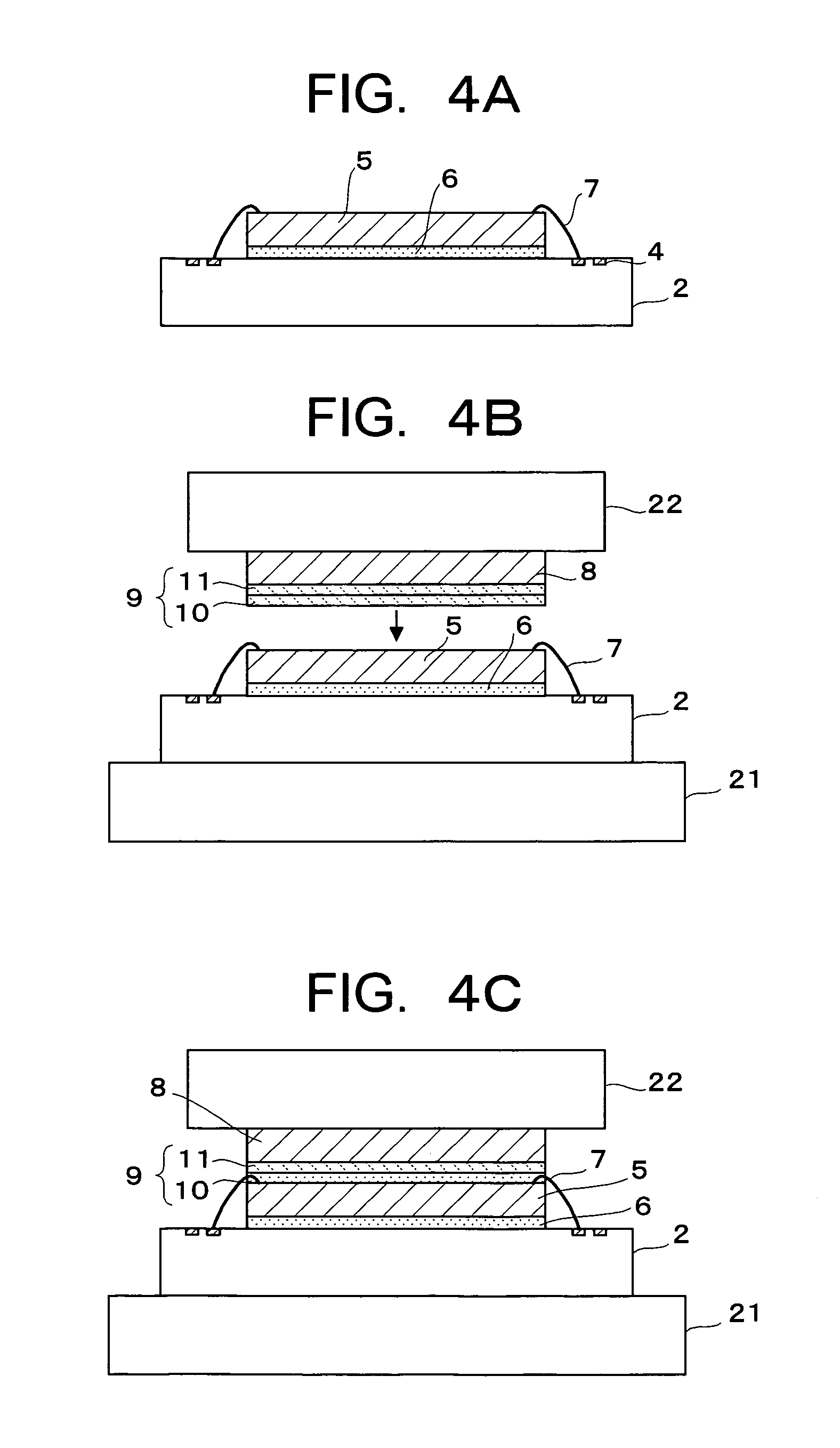
[0112] The above-stated semiconductor device 70 of the fifth embodiment is created, for example, as described below. The manufacturing process of the semiconductor device 70 is described with reference to FIG. 26A to FIG. 26D. At first, as shown in FIG. 26A, the first semiconductor element 5 is adhered on the circuit board 2 by using the first adhesive layer 6. Subsequently, the wire bonding process is performed, and the electrode portions 4 of the circuit board 2 and the electrode pads of the first semiconductor element 5 are electrically connected by the first bonding wires 7.

[0113] Next, as shown in FIG. 26B, the insulating columnar bodies 73 are formed at predetermined positions of the circuit board 2 to which the first semiconductor element 5 is adhesive mounted. The insulating column body 73 is formed by coating the thermosetting insulating resin such as the epoxy resin, the light curing insulating resin, and so on, in column state as stated above. The insulating columnar body...


PUM


Abstract

A stacked electronic component comprises a first electronic component adhered on a substrate via a first adhesive layer, and a second electronic component adhered by using a second adhesive layer thereon. The second adhesive layer has a two-layer structure formed by a same material and having different modulus of elasticity. The second adhesive layer of the two-layer structure has a first layer disposed at the first electronic component side and a second layer disposed at the second electronic component side. The first layer softens or melts at an adhesive temperature. The second layer maintains a layered shape at the adhesive temperature. According to the stacked electronic component, occurrences of an insulation failure and a short circuiting are prevented, and in addition, a peeling failure between the electronic components, an increase of a manufacturing cost, and so on, can be suppressed.

Description

CROSS-REFERENCE TO THE INVENTION [0001] This application is based upon and claims the benefits of priorities from the prior Japanese Patent Application No. 2004-150046 and Japanese Patent Application No. 2004-150047, filed on May 20, 2004; the entire contents of which are incorporated herein by reference. BACKGROUND [0002] 1. Field of the Invention [0003] The present invention relates to a stacked electronic component constituted by stacking a plurality of electronic components, and a manufacturing method thereof. [0004] 2. Description of the Related Art [0005] Recently, to realize a miniaturization and a high-density mounting, and so on, of semiconductor devices, a stacked-type multi chip package in which a plurality of semiconductor elements (semiconductor chip) are stacked and sealed in one package is put into practical use. In the stacked-type multi chip package, the plurality of semiconductor elements are stacked sequentially on a circuit board via an adhesive such as a die att...

Claims


Application Information

Patent Timeline
IPC IPC(8): H05K7/00
CPCH01L23/49575H01L2224/32145H01L2224/32225H01L2224/48091H01L2224/48227H01L2224/73265H01L2225/0651H01L2225/06555H01L2225/06562H01L2225/06575H01L2225/06586H01L2924/09701H01L2924/15311H01L25/0657H01L2924/19107H01L2224/92247H01L2224/48247H01L2224/32245H01L25/03H01L2924/00014H01L2924/00H01L2924/00012H01L2224/49H01L2924/181H01L24/73H01L24/48H01L2224/45099H01L2224/05599H01L23/3107H01L24/33H01L24/49
Inventor YOSHIMURA, ATSUSHIKOMUTA, NAOYUKINUMATA, HIDEO
Owner KIOXIA CORP
Why Eureka
Try Eureka