Method of producing a complex structure by assembling stressed structures

a stress-strength, complex structure technology, applied in the direction of medical science, application, lamination, etc., can solve the problems of high internal stress within the heterostructure, step changes necessitate large changes in temperature, damage or even destroy the complex structure, etc., to achieve good quality, improve mechanical stability, and control accurately

Active Publication Date: 2006-06-29
COMMISSARIAT A LENERGIE ATOMIQUE ET AUX ENERGIES ALTERNATIVES
View PDF10 Cites 43 Cited by
  • Summary
  • Abstract
  • Description
  • Claims
  • Application Information

AI Technical Summary

Benefits of technology

[0012] Moreover, the invention produces an autonomous epitaxial growth support in the form of a stressed complex structure suitable for a given material to be grown epitaxially. Because of the internal stresses generated within this structure during assembly, and more particularly surface stresses, the surface lattice parameter can be controlled accurately with no device other than the other portion of the complex structure. Thus epitaxial growth of good quality can be obtained using this stressed complex structure.
[0013] It is to be noted that, in an entirely different context, the paper by D. Feijoo, I. Ong, K. Mitani, W. S. Yang, S. Yu and U. M. Gösele, “Prestressing of bonded wafers”, Proceedings of the 1st international symposium on semiconductor wafer bonding, science technology and applications, Vol. 92-7, The Electrochemical Society (1992) page 230, proposes a method of generating internal stresses within a complex structure, but this is not to address either of the two problems as stated, but rather with a view to improving the mechanical stability of the structure.

Problems solved by technology

Now, most of these steps necessitate large changes in temperature.
The change of temperature can generate high internal stresses within the heterostructure because the materials change differently with temperature.
If the stresses are too high, they can damage or even destroy the complex structure.
There therefore remains the problem of producing a complex structure reliably and reproducibly by assembling two different materials so that the structure is able, without risk, to withstand technology steps at higher temperatures or of longer duration than those to which the art is currently limited.
Another major problem in microelectronics is that of being able to produce good quality epitaxially grown material of a given kind on another material.
In this case, the problem lies in the possible difference between the lattice parameters of the two materials, i.e. that of the substrate and that to be grown epitaxially.
For example, if Si0.8Ge0.2 is to be grown epitaxially on silicon, the lattice difference between these two materials is so large that it is not possible to grow an Si0.8Ge0.2 layer of more than a few hundred angstrom units thickness before the layer relaxes and forms numerous dislocations that are very harmful to crystal quality.
However, it is not immediately apparent how to exploit this fact to produce epitaxial growth of high quality because, without modifying the epitaxial growth plant, how can it be possible to produce an epitaxially grown substrate with a matched lattice parameter from a given unsuitable substrate, and how can this be achieved accurately and reproducibly?

Method used


Image

  • Method of producing a complex structure by assembling stressed structures
  • Method of producing a complex structure by assembling stressed structures
  • Method of producing a complex structure by assembling stressed structures

Examples


Embodiment Construction

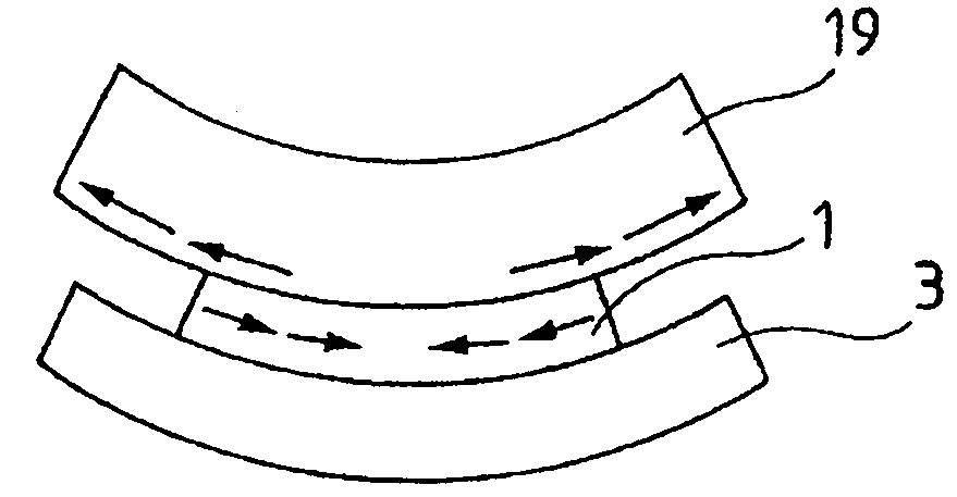
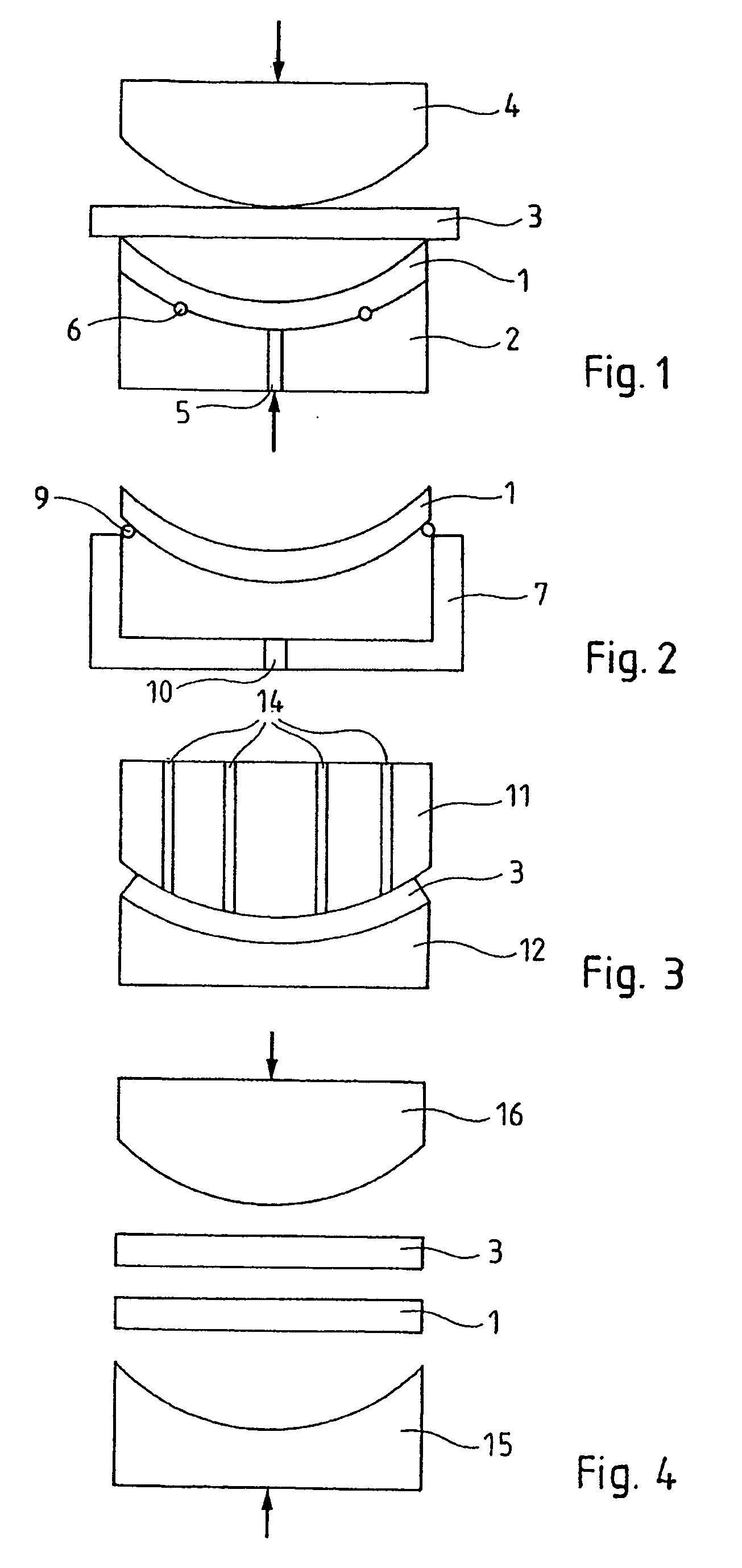
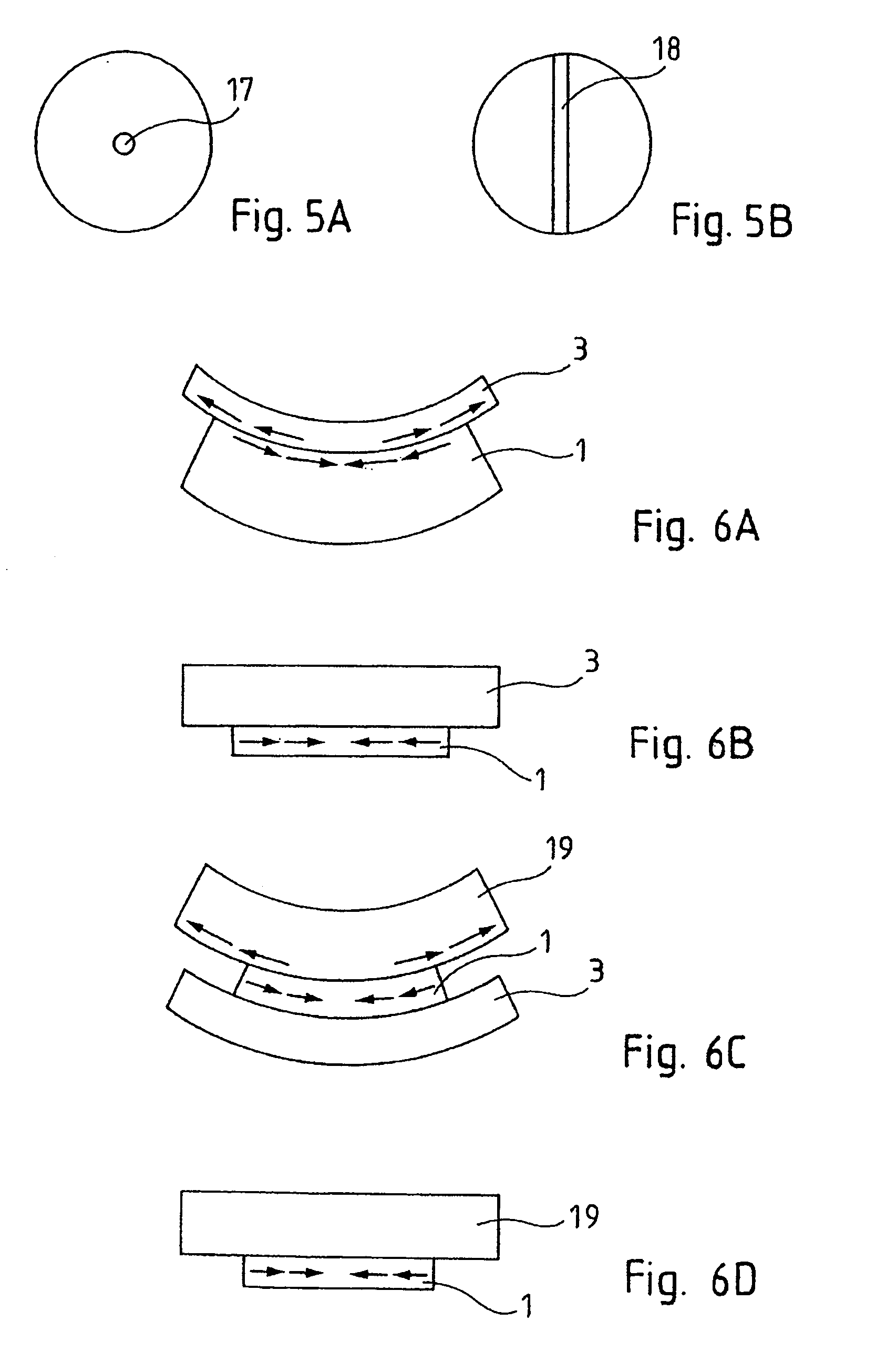
[0060] Curved Bonding

[0061] In the figures to which the following description refers, identical, similar or equivalent parts are identified by the same reference numbers. Also, to clarify the figures, the various items are not represented to a consistent scale.

[0062]FIG. 1 shows one non-limiting embodiment of the invention. A first basic structure 1 is deformed by aspirating it onto a first preform 2 of specific shape, for example of spherical concave shape. Aspiration is effected by means of aspiration channels 5 opening onto the surface of the preform. Seals 6 at the periphery of the preform support the first structure 1 and ensure a pressure difference is obtained between the two faces of that structure. Because of this pressure difference, the structure is deformed to espouse the shape of the first preform 2. Because of this deformation, stresses familiar to and quantifiable by the person skilled in the art are generated within the first structure 1 and in particular at its ex...


PUM

PropertyMeasurementUnit
thicknessaaaaaaaaaa
diameteraaaaaaaaaa
thickaaaaaaaaaa

Abstract

The invention relates to a method of producing a complex microelectronic structure, in which two basic microelectronic structures (1, 3) are assembled at the two respective connecting faces (3) thereof. The invention is characterised in that, before assembly, a difference is created in the tangential stress state between the two faces to be assembled, said difference being selected such as to produce a pre-determined stress state within the assembled structure under given conditions in relation to the assembly conditions.

Description

TECHNICAL FIELD [0001] The invention relates to a method of producing a complex structure by assembling two basic microelectronic structures. The structures may be microelectronic, microtechnological, nanotechnological or nanoelectronic. [0002] The use of these complex structures, and in particular those obtained by assembling structures of different materials, is increasingly widespread in microelectronics, for highly diverse reasons. For example, these complex structures, also known as heterostructures, reduce costs by avoiding the use of costly solid (for example silicon carbide) substrates. In the case of an SOI (silicon on insulator) substrate, for example, they also facilitate isolating components from each other, thereby increasing the integration density, limiting component consumption, increasing speed, etc. DESCRIPTION OF THE PRIOR ART [0003] To be advantageous, these complex structures must be compatible, subject to minor modifications, with the standard technology steps ...

Claims


Application Information

Patent Timeline
Patent Type & Authority Applications(United States)
IPC IPC(8): H01L21/46H01L21/18H01L21/20H01L21/68H01L21/762
CPCH01L21/187H01L21/2007H01L2924/10253H01L21/67092H01L21/6835H01L21/76251H01L2221/68363H01L2924/3511H01L24/75H01L2924/01029Y10S148/012Y10S148/159Y10S148/135H01L2924/00H01L21/20
Inventor FOURNEL, FRANCKMORICEAU, HUBERTMONTMAYEUL, PHILIPPE
Owner COMMISSARIAT A LENERGIE ATOMIQUE ET AUX ENERGIES ALTERNATIVES
Why Eureka
Try Eureka