Liquid crystal display device

a liquid crystal display and display device technology, applied in non-linear optics, instruments, optics, etc., can solve the problems of slow process of liquid crystal material, slow injection of liquid crystal material between the two substrates, lowering yield, etc., to reduce the variation of thickness, reduce the contact area, and reduce the effect of cell gap stability

Active Publication Date: 2006-07-06
LG DISPLAY CO LTD +1
View PDF11 Cites 16 Cited by
  • Summary
  • Abstract
  • Description
  • Claims
  • Application Information

AI Technical Summary

Benefits of technology

[0038] An advantage of the present invention is to provide an LCD device in which column spacers for a cell gap are arranged between gate and data lines to reduce a contact area between the column spacers and an opposing substrate and a stable cell gap is maintained over the whole panel by reducing variation of a thickness per area of a thin film transistor (TFT) substrate corresponding to the column spacers.
[0039] Additional advantages, and features of the invention will be set forth in part in the description which follows and in part will become apparent to those having ordinary skill in the art upon examination of the following or may be learned from practice of the invention. The advantages of the invention may be realized and attained by the structure particularly pointed out in the written description and claims hereof as well as the appended drawings.
[0040] To achieve these and other advantages and in accordance with the purpose of the invention, as embodied and broadly described herein, an LCD device according to the present invention includes first and second substrates facing ea

Problems solved by technology

This kind of LCD device is referred to as a twisted nematic (TN) mode LCD device, which has disadvantageous characteristics such as a narrow viewing angle.
However, the method of manufacturing the LCD device by the liquid crystal injection method has the following disadvantages.
The process of injecting liquid crystal material between the two substrates is slow thereby lowering yield.
Also in the case of forming a large sized LCD device, it is difficult to completely inject the liquid crystal material into the inside of the LCD panel, thereby causing failure due to incomplete injection of the liquid crystal material.
Furthermore, the process of the liquid crystal material is slow and a large space is required for the liquid crystal injection device.
In this method, it is impossible to use ball spacers for maintaining a cell gap between the two substrates since the ball spacers move in the spreading direction of liquid crystal material.
As described above, the LCD device including the column spacers has a relatively large contact area with an opposing substrate (TFT substrate) unlike the ball spacers, thereby causing a great frictiona

Method used


Image

  • Liquid crystal display device
  • Liquid crystal display device
  • Liquid crystal display device

Examples


first embodiment

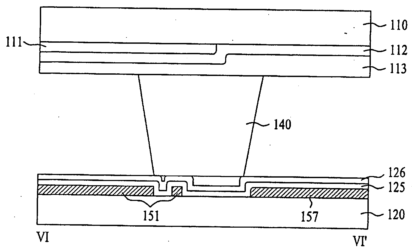
[0107]FIG. 10 is a plan view illustrating an LCD device according to the present invention, FIG. 11A is a structural sectional view taken along line III-III′ of FIG. 10, and FIG. 11B is a structural sectional view taken along line IV-IV′ of FIG. 10.

[0108] As shown in FIG. 10, FIG. 11A and FIG. 1B, the LCD device according to the first embodiment of the present invention includes first and second substrates 110 and 120 facing each other and bonded to each other, and a liquid crystal layer (not shown) filled between the two substrates.

[0109] In more detail, the first substrate 110 includes a black matrix layer 111 shielding light from portions (regions for gate and data lines and TFT) except for pixel regions, an R / G / B color filter layer 112 formed to correspond to the pixel regions, thereby displaying colors, and an overcoat layer 113 formed on an entire surface of the black matrix layer 111 and the color filter layer 112.

[0110] The second substrate 120 includes a plurality of gate...

second embodiment

[0137]FIG. 12 is a plan view illustrating a first column spacer of an LCD device according to the present invention.

[0138] As shown in FIG. 12, the first column spacer 140 of the LCD device according to the second embodiment of the present invention is arranged between the gate line 131 and the common line 137, which are more adjacent to each other than those of the first embodiment. The column spacer 140 is overlapped with the upper portion on the gate and common lines. In this case, to maintain the contact area between the second substrate 120 and the first column spacer 140 similarly to the first embodiment, the line width can be reduced so that the gate line 131 and the common line 137 below the first column spacer 140 can be more retracted.

third embodiment

[0139]FIG. 13 is a plan view illustrating a first column spacer of an LCD device according to the present invention, and FIG. 15 is a structural sectional view taken along line V-V′ of FIG. 13.

[0140] As shown in FIG. 13 and FIG. 15, in the LCD device according to the third embodiment of the present invention, a gate line 142 and a common line 147 are formed on a second substrate in parallel with each other. The gate line 142 and the common line 147 are respectively provided with a gate slit 142a and a common slit 147a to face each other. The first column spacer 140 is formed on the first substrate between the gate slit 142a and the common slit 147a.

[0141] At this time, the first column spacer 140 is formed on the line V-V′ of FIG. 13. That is, the first column spacer 140 is formed over the gate line 142, the gate slit 142a, the gate line, the common line 147, and the common slit 147a and the common line 147. The first column spacer 140 may be extended to the gate slit 142a and the ...


PUM


Abstract

An LCD device is disclosed in which column spacers for a cell gap are arranged between gate and common lines to reduce a contact area between the column spacers and an opposing substrate, and a stable cell gap is maintained over the whole panel by reducing variation of a thickness per area of a thin film transistor (TFT) substrate corresponding to the column spacers. The LCD device includes first and second substrates facing each other, gate and data lines formed on the first substrate to cross each other, and pixel regions, a thin film transistor formed in each portion where the gate and data lines cross, common and pixel electrodes alternately formed in the pixel regions, common lines formed adjacent to the gate lines substantially parallel to the gate lines, a first column spacer formed on the second substrate corresponding to a portion between the gate line and the common line, and a liquid crystal layer filled between the first and second substrates.

Description

[0001] This application claims the benefit of the Korean Patent Application No. 10-2004-116284, filed on Dec. 30, 2004, which is hereby incorporated by reference for all purposes as if fully set forth herein. BACKGROUND OF THE INVENTION [0002] 1. Field of the Invention [0003] The present invention relates to a liquid crystal display (LCD) device, and more particularly, to an LCD device in which column spacers for a cell gap are arranged between gate and common lines to reduce a contact area between the column spacers and an opposing substrate, and a stable cell gap is maintained over the whole panel by reducing variation of a thickness per area of a thin film transistor (TFT) substrate corresponding to the column spacers. [0004] 2. Discussion of the Related Art [0005] A related art LCD device will be described with reference to the accompanying drawings. [0006]FIG. 1 is an exploded perspective view illustrating a related art LCD device. [0007] As shown in FIG. 1, the related art LCD...

Claims


Application Information

Patent Timeline
IPC IPC(8): G02F1/1333
CPCG02F1/13394G02F1/134363G02F1/1339
Inventor KIM, JONG WOOYOO, WON HYUNG
Owner LG DISPLAY CO LTD
Why Eureka
Try Eureka