Liquid crystal display device and fabricating method thereof

Active Publication Date: 2006-07-06
LG DISPLAY CO LTD
View PDF12 Cites 46 Cited by
  • Summary
  • Abstract
  • Description
  • Claims
  • Application Information

AI Technical Summary

Benefits of technology

[0012] Accordingly, an advantage of the present invention is to provide a thin film transistor substrate of an EL display panel with a simplified structure and a method of fabricating the same.
[0013] Additional features and advantages of the invention will be set forth in the description which follows, and in part will be apparent from the description, or may be learned by practice of the invention. The objectives and other advantages of the invention will be realized and attained by the structure particularly pointed out in the written description and claims thereof as well as the appended drawings.
[0014] To achieve these and other advantages and in accordance with the purpose of the present invention, as embodied and broadly described, there is provided a liquid crystal display device, comprising: a first thin film transistor having an active layer, a gate electrode with a double layer structure overlapping the poly active layer with a gate insulating film there between, a source electrode and a drain electrode connected to the active layer through first and second contact holes which penetrate an interlayer insulating film on the gate insulating film; a pixel electrode having a double layer structure, including a first transparent conductive layer and a second conductive layer, formed on the gate insulating film, wherein a portion of the first transparent conductive layer is exposed through a first transmission hole, which penetrates the interlayer insulating film; a luminance layer on a portion of the pixel electrode; and a common electrode formed on the luminance layer.
[0015] In another aspect of the present invention, there is provided a method of fabricating a liquid crystal display device, comprising: forming an active layer on a substrate; forming a gate insulating film on the active layer; forming a double layer pattern including a pixel electrode and a gate electrode, the gate electrode overlapping the active layer; forming a source area and a drain area by

Problems solved by technology

In the related art organic EL display panel, a thin film transistor substrate is formed by a plurality of mask proce

Method used


Image

  • Liquid crystal display device and fabricating method thereof
  • Liquid crystal display device and fabricating method thereof
  • Liquid crystal display device and fabricating method thereof

Examples


Embodiment Construction

[0024] Reference will now be made in detail to embodiments of the present invention, examples of which are illustrated in the accompanying drawings.

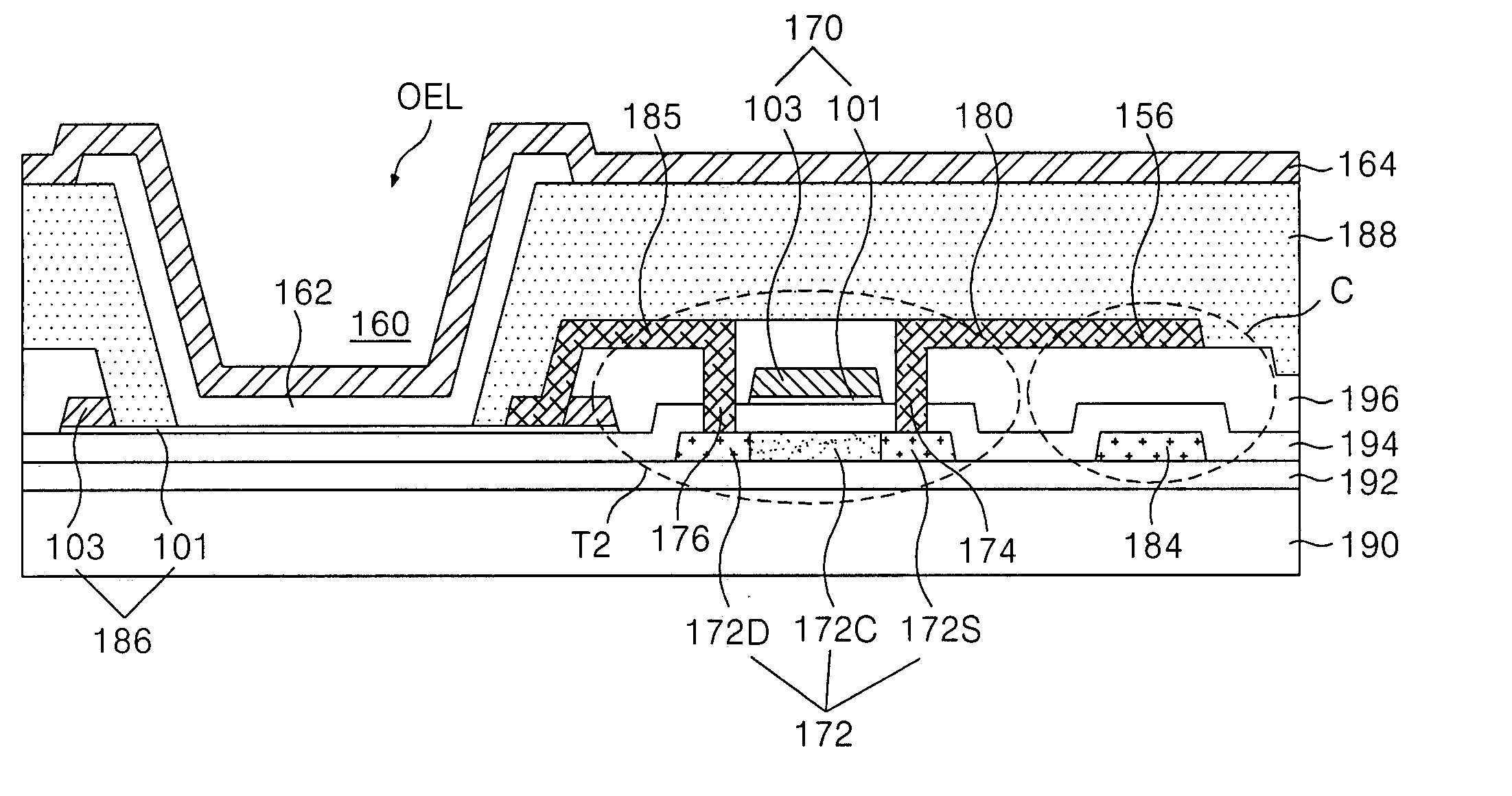
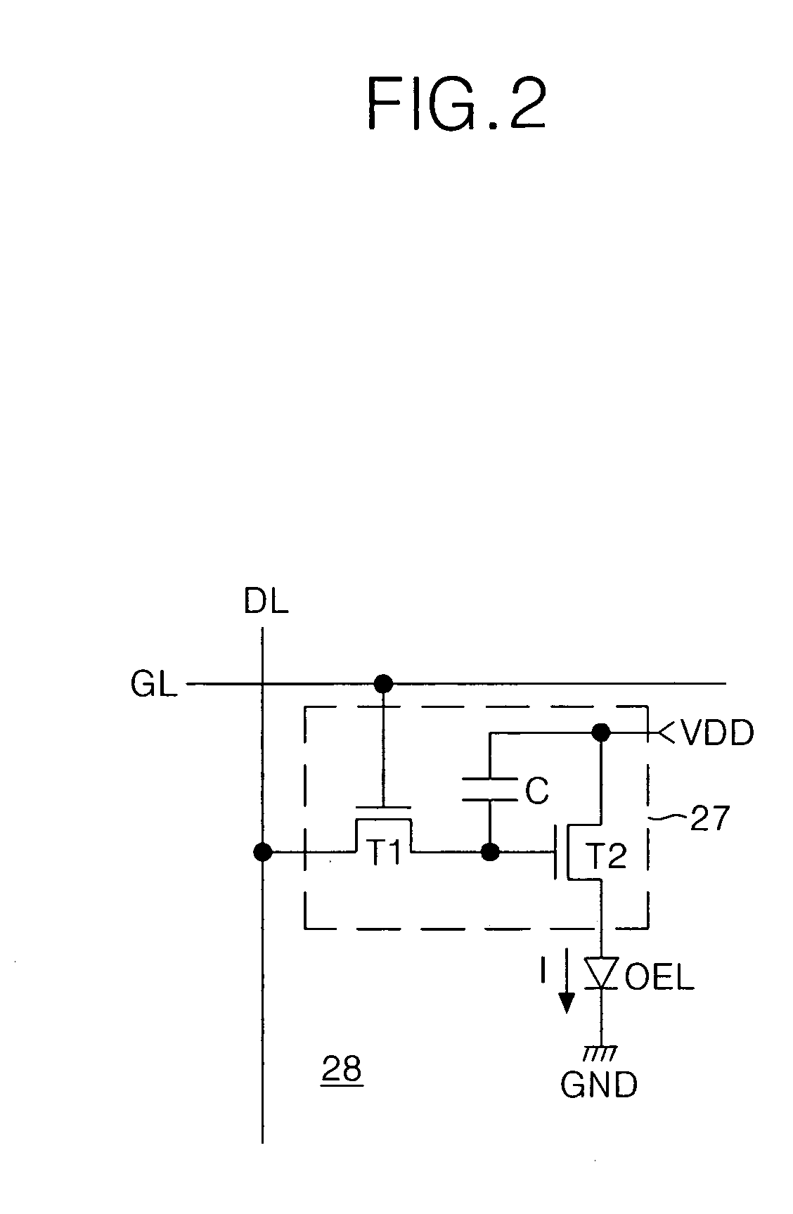
[0025]FIG. 2 is an equivalent circuit diagram of a pixel which is included in a thin film transistor substrate of an organic EL panel according to an embodiment of the present invention, and FIG. 3 is a sectional diagram illustrating a vertical structure of a storage capacitor C, a drive thin film transistor T2 and an EL cell (OEL) in the pixel 28 illustrated in FIG. 2.

[0026] Referring to FIG. 2, the pixel 28 includes a cell driver 27 connected to a gate line GL and a data line DL, and an EL cell (OEL) connected to the cell driver 27. The cell driver 27 includes a switch thin film transistor T1 connected to the gate line GL and the data line DL; a drive thin film transistor T2 connected between the switch thin film transistor T1, a supply voltage source VDD and an anode of the EL cell (OEL); and a storage capacitor C connected between ...


PUM


Abstract

A liquid crystal display device includes a first thin film transistor having an active layer, a gate electrode with a double conductive layer structure overlapping the active layer with a gate insulating film there between, a source electrode and a drain electrode connected to the active layer through first and second contact holes which penetrate an interlayer insulating film on the gate insulating film; a pixel electrode having a double layer structure, including a first transparent conductive layer and a second conductive layer, formed on the gate insulating film, wherein a portion of the first transparent conductive layer is exposed through a first transmission hole, which penetrates the interlayer insulating film; a luminescence layer on a portion of the pixel electrode; and a common electrode on the luminescence layer.

Description

[0001] This application claims the benefit of the Korean Patent Application No. 2004-118560, filed on Dec. 31, 2004, which is hereby incorporated by reference for all purposes as if fully set forth herein. BACKGROUND OF THE INVENTION [0002] 1. Field of the Invention [0003] The present invention relates to an electro-luminescence display panel, and more particularly to a simplified structure and process of making a thin film transistor array of an EL display panel. [0004] 2. Description of the Related Art [0005] Various flat panel display devices have been developed which overcome the weight and size disadvantages of a cathode ray tube (CRT) display device. These flat panel display devices include liquid crystal display (LCD) devices, field emission display (FED) devices, plasma display panel (PDP) devices, and electro-luminescence (EL) display panel devices. [0006] The EL display panel is a self luminous device which makes phosphorus emit light by re-combining electrons and holes. A...

Claims


Application Information

Patent Timeline
IPC IPC(8): C09K19/00H05B44/00
CPCH01L27/1214H01L27/3248Y10T428/10H01L2227/323H01L27/1288H01L51/56C09K2323/00H10K59/123H10K59/1201H10K71/00H05B33/00H05B33/10H05B33/26
Inventor PARK, YONG IN
Owner LG DISPLAY CO LTD
Why Eureka
Try Eureka