Method of fabricating chrome-less phase shift mask

a phase shift mask and phase shift technology, applied in the field of photo masks, can solve the problems of difficult to achieve a high accuracy of the circuit pattern with the chrome mask, the limitation of forming a fine-sized circuit pattern with the photo mask using the chrome light-shielding film, and the inherently caused error of the chrome mask

Inactive Publication Date: 2006-07-06
SAMSUNG ELECTRONICS CO LTD
View PDF5 Cites 3 Cited by
  • Summary
  • Abstract
  • Description
  • Claims
  • Application Information

AI Technical Summary

Benefits of technology

[0012] The present invention has been made to solve the aforementioned problems. The present invention is directed to provide a method of fabricating a chrome-less phase shift mask capable of expanding a patternable region.

Problems solved by technology

The chrome mask inherently has an error caused by light diffraction.
That is, it is difficult to achieve a high accuracy of the circuit pattern with the chrome mask.
Accordingly, the photo mask using the chrome light-shielding film has limitations in forming a fine-sized circuit pattern.
Light sources having a mutual phase difference of 180° cause interference.
This limits the use of the chrome-less phase shift mask, complicates the fabrication process, and degrades patterning accuracy in a non-patternable region.

Method used


Image

  • Method of fabricating chrome-less phase shift mask
  • Method of fabricating chrome-less phase shift mask
  • Method of fabricating chrome-less phase shift mask

Examples


Embodiment Construction

[0017] The present invention will now be described more fully hereinafter with reference to the accompanying drawings, in which preferred embodiments of the invention are shown. This invention may, however, be embodied in many different forms and should not be construed as being limited to the embodiments set forth herein. Rather, these embodiments are provided so that this disclosure will be thorough and complete, and will fully convey the scope of the invention to those skilled in the art. In the drawings, the thicknesses of layers and regions are exaggerated for clarity. Like numbers refer to like elements throughout the specification.

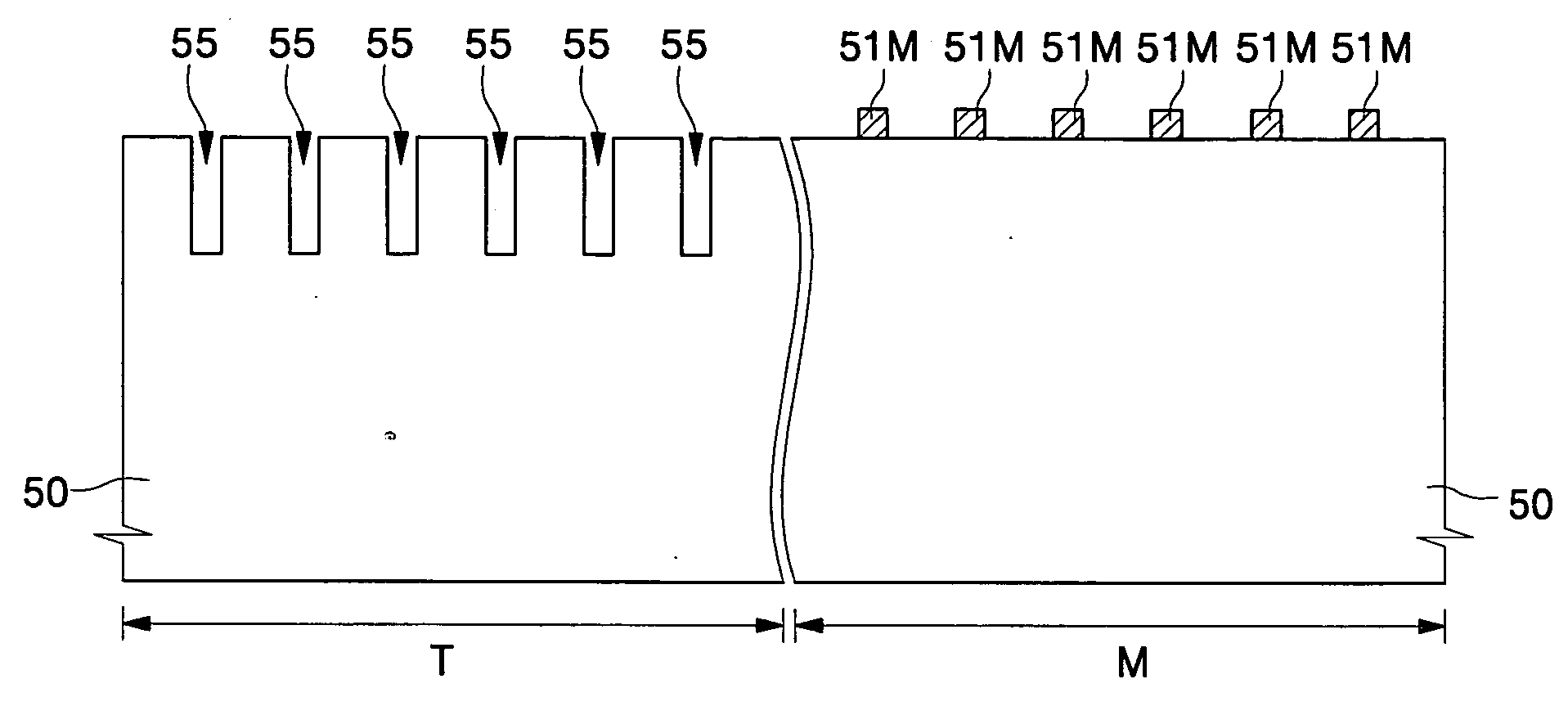
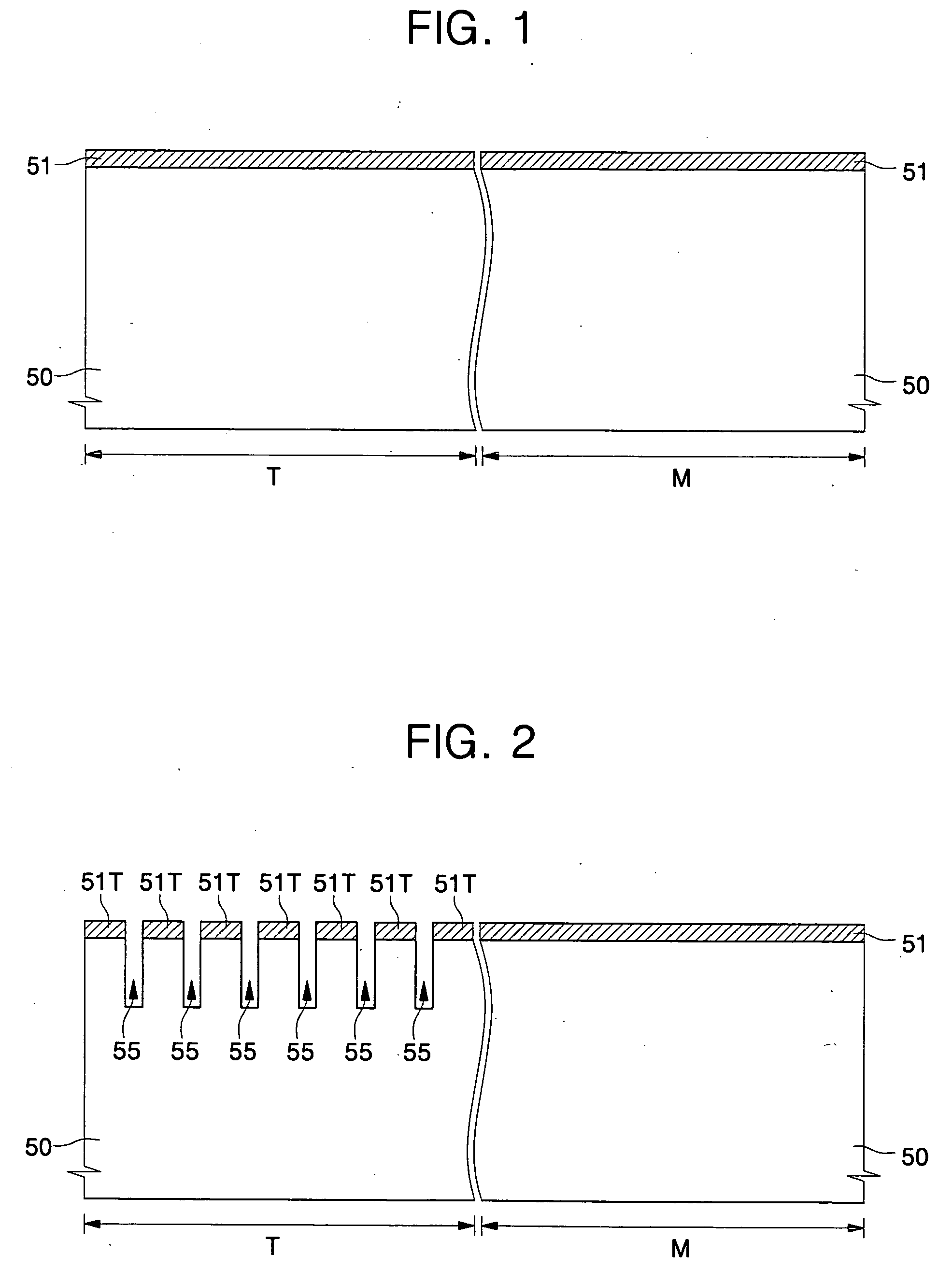
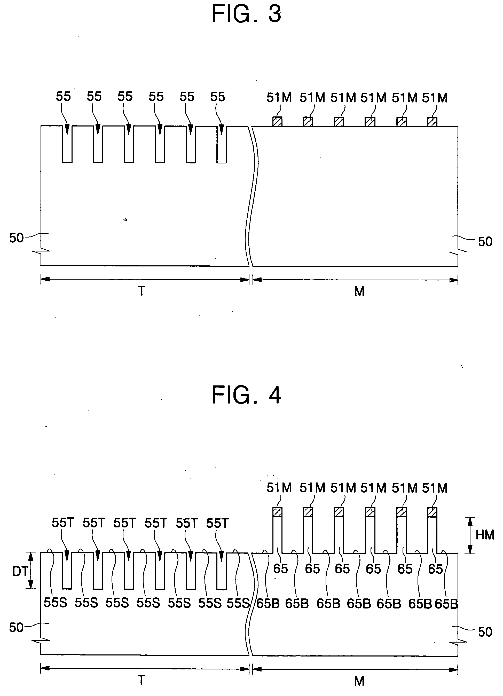
[0018] FIGS. 1 to 5 are cross-sectional views illustrating a method of fabricating a chrome-less phase shift mask according to an embodiment of the present invention.

[0019] Referring to FIG. 1, a hard mask film 51 is formed on a surface of a mask body 50 having a trench circuit area T and a mesa circuit area M.

[0020] The mask body 50 may be forme...


PUM

PropertyMeasurementUnit
wavelengthaaaaaaaaaa
areaaaaaaaaaaa

Abstract

An embodiment of a method of fabricating a chrome-less phase shift mask includes forming a hard mask film on a surface of a mask body having a trench circuit area and a mesa circuit area. The hard mask film is patterned. The mask body is anisotropically etched using the hard mask pattern as an etching mask to form pre-pitting patterns in the trench circuit area. The hard mask film having the hard mask pattern is again patterned to form a mesa hard mask pattern on the mesa circuit area and to expose a top surface of the trench circuit area. The mask body is anisotropically etched to form phase shift hillock patterns in the mesa circuit area and phase shift pitting patterns in the trench circuit area. Phase shift pitting patterns and phase shift hillock patterns may be formed on a single body.

Description

CROSS-REFERENCE TO RELATED APPLICATION [0001] This application claims priority from Korean Patent Application No. 2005-00994, filed Jan. 5, 2005, the disclosure of which is hereby incorporated herein by reference in its entirety as is set forth fully herein. BACKGROUND OF INVENTION [0002] 1. Technical Field [0003] The present invention relates to a method of fabricating a photo mask, and more particularly, to a method of fabricating a chrome-less phase shift mask having no light-shielding film formed of chrome. [0004] 2. Discussion of the Related Art [0005] Among processes for semiconductor fabrication, a photolithographic process of forming a fine circuit on a semiconductor substrate is critical. The productivity and quality of a semiconductor device depend on the process capability of the photolithographic process. In the photolithographic process, a photo mask is used to form a given circuit pattern on a semiconductor substrate. A chrome mask is an example of a photo mask. The ch...

Claims


Application Information

Patent Timeline
Patent Type & Authority Applications(United States)
IPC IPC(8): G03C5/00G03F1/00
CPCG03F1/34G03F1/26
Inventor YOON, GI-SUNGSHIN, IN-KYUNKIM, SUNG-HYUCK
Owner SAMSUNG ELECTRONICS CO LTD
Why Eureka
Try Eureka