

Interconnection structure having double diffusion barrier layer and method of fabricating the same
a diffusion barrier layer and interconnection technology, applied in the direction of semiconductor devices, semiconductor/solid-state device details, chairs, etc., can solve the problems of affecting device characteristics, difficult to pattern the copper layer using a typical photolithography process, and the deterioration of the low-k characteristics of the interlayer insulating layer,
- Summary
- Abstract
- Description
- Claims
- Application Information
AI Technical Summary
Benefits of technology
Problems solved by technology
Method used
Image

Examples
Embodiment Construction
[0031] The present invention will now be described more fully hereinafter with reference to the accompanying drawings, in which preferred embodiments of the invention are shown. This invention may, however, be embodied in many different forms and should not be construed as being limited to the embodiments set forth herein. In the drawings, the thicknesses of layers and regions are exaggerated for clarity. Like numbers refer to like elements throughout the specification.
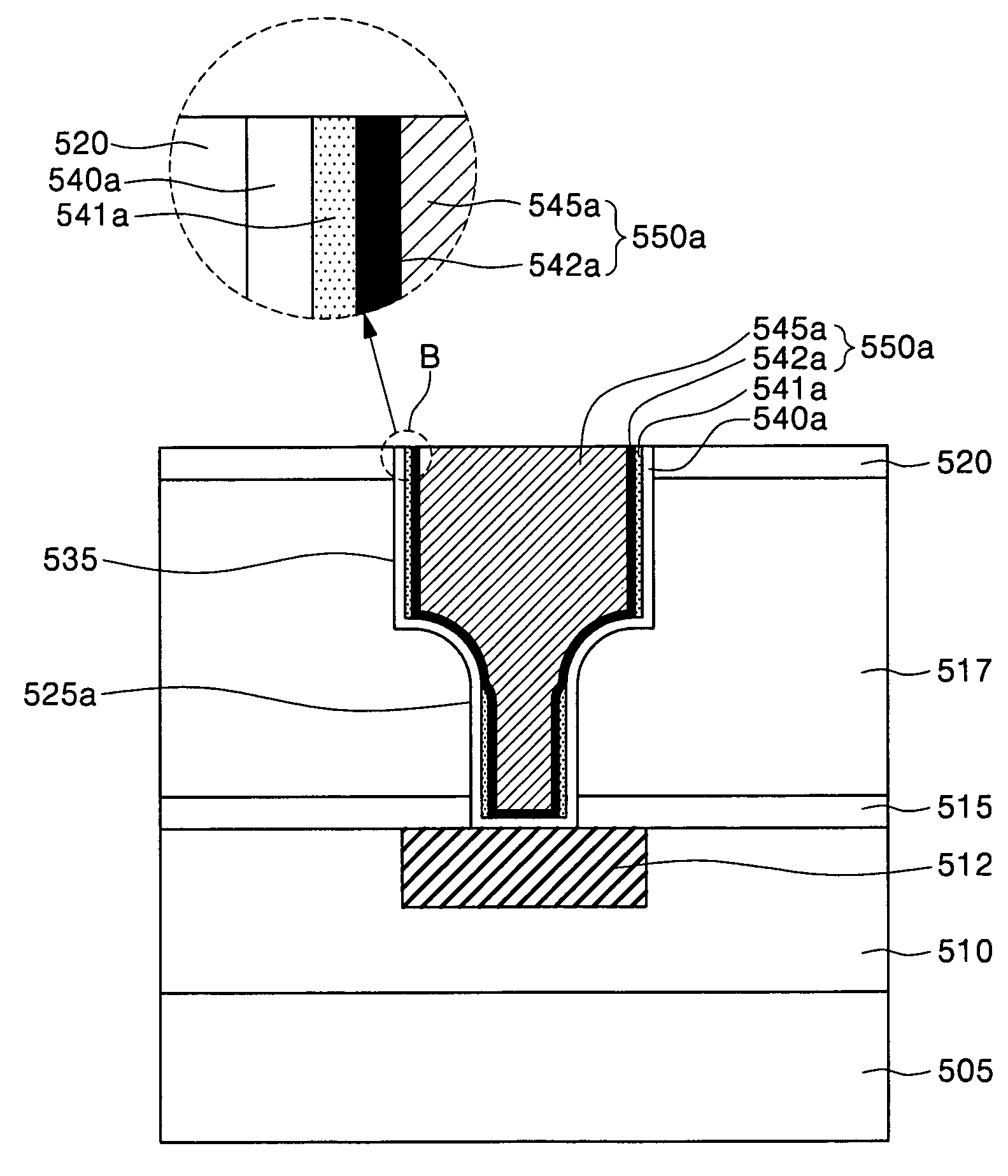
[0032]FIG. 4 is a process flow chart illustrating a method of fabricating an interconnection structure having a double diffusion barrier layer according to an exemplary embodiment of the present invention, and FIGS. 5A to 5I are sectional views illustrating a method of fabricating an interconnection structure having a double diffusion barrier layer according to an exemplary embodiment of the present invention.
[0033] Referring to FIGS. 4 and 5A, a lower insulating layer 510 is formed on a semiconductor substrate 505....
PUM
 Abstract
Description
Claims
Application Information