

Semiconductor Device and Method for Fabricating the Same
a technology of semiconductor devices and semiconductors, applied in the direction of semiconductor devices, electrical equipment, transistors, etc., can solve the problems of mismatch characteristics, poor hot carrier injection (hci) of cmos devices having a conventional ldd structure, and poor heat transfer characteristics of cmos devices
- Summary
- Abstract
- Description
- Claims
- Application Information
AI Technical Summary
Benefits of technology
Problems solved by technology
Method used
Image

Examples
Embodiment Construction
[0017]Reference will now be made in detail to the specific embodiments of the present invention, examples of which are illustrated in the accompanying drawings. Wherever possible, the same reference numbers will be used throughout the drawings to refer to the same or like parts.
[0018]A semiconductor device in accordance with embodiments of the present invention is described below in reference to FIG. 6.
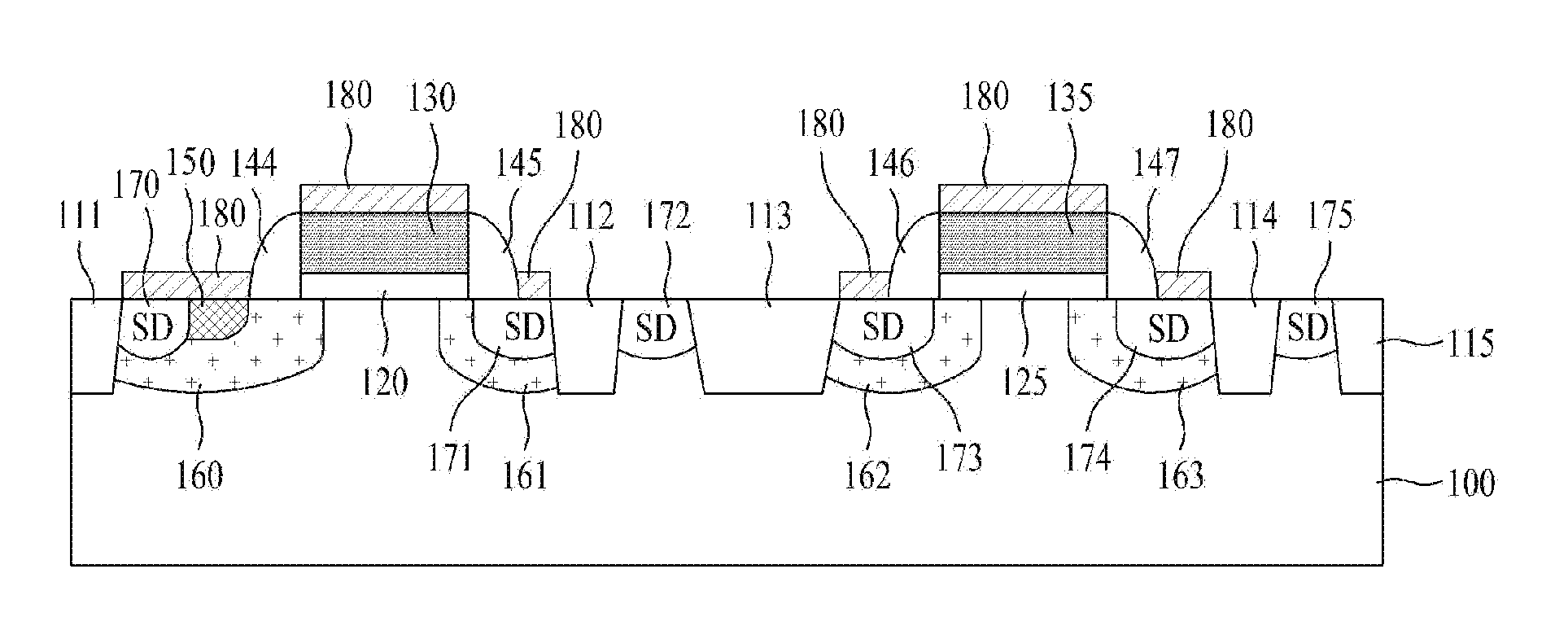
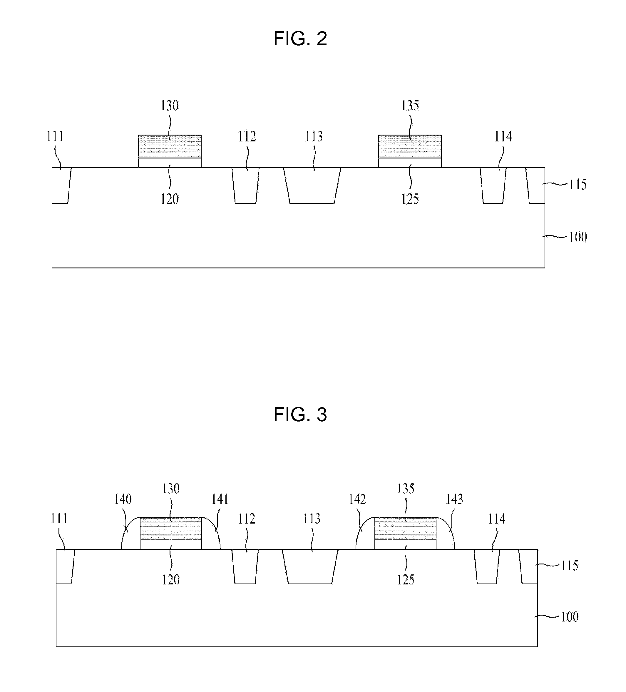
[0019]The semiconductor device has shallow trench isolation (STI) structures for isolating N-wells or P-wells in a P-type or N-type semiconductor substrate (which may be a single crystalline semiconductor substrate, or a single-crystal silicon wafer with one or more layers of epitaxial silicon grown thereon).
[0020]The semiconductor device includes gate oxide films 120 and 125, gate electrodes 130 and 135, double diffusion drain region 150, double diffusion junction regions 160, 161, 162, and 163, and source / drain regions 170, 171, 172, 173, 174, and 175.
[0021]The double diffusion junc...
PUM
 Abstract
Description
Claims
Application Information