Consumption type N-type lateral double-diffusion metal-oxide semiconductor for reducing voltage

A lateral double diffusion, semiconductor tube technology, applied in the direction of semiconductor devices, electrical components, circuits, etc., can solve the problems of inability to drive circuits, small current capacity, low breakdown voltage, etc., to achieve simple circuit architecture, enhanced freedom, and preparation. Craft Compatible Effects

Active Publication Date: 2011-02-09
SOUTHEAST UNIV
View PDF3 Cites 18 Cited by
  • Summary
  • Abstract
  • Description
  • Claims
  • Application Information

AI Technical Summary

Problems solved by technology

[0004] In related technologies, few people pay attention to depletion-type high-voltage lateral double-diffused metal-oxide-semiconductor transistors. The threshold voltage of traditional depletion-type high-voltage lateral double-diffused metal-oxide semiconductor transistors only depends on the polysilicon gate to deplete the channel implantation region. However, due to the limitation of the depletion capacity, the threshold voltage of the depletion of the traditional structure is distributed between -1 and -3V. Finally, the low-voltage power supply obtained after the depletion is stepped down cannot drive the low-voltage part

Method used


Image

  • Consumption type N-type lateral double-diffusion metal-oxide semiconductor for reducing voltage
  • Consumption type N-type lateral double-diffusion metal-oxide semiconductor for reducing voltage
  • Consumption type N-type lateral double-diffusion metal-oxide semiconductor for reducing voltage

Examples


Embodiment Construction

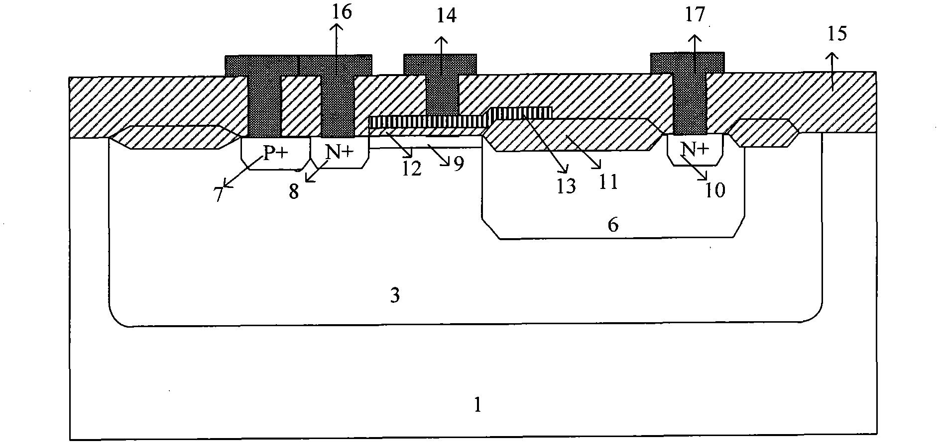
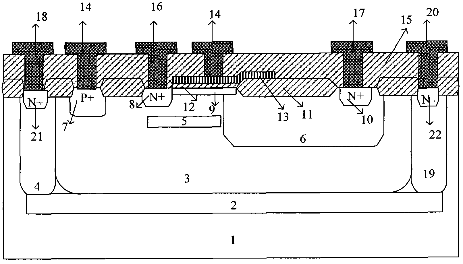
[0021] Reference image 3 , A depletion-type N-type lateral double-diffusion metal oxide semiconductor tube for step-down, comprising: a P-type semiconductor substrate 1, on which an N-type buried layer 2 is provided, and an N-type buried layer 2 is provided with a P-type well region 3, on the left and right sides of the P-type well region 3 are respectively provided with a first N-type well region 4 and a second N-type well region 19 forming a PN junction isolation, in the first N-type well The region 4 is provided with a first N-type ohmic contact region 21, a second N-type ohmic contact region 22 is provided on the second N-type well region 19, and a drain terminal N-type drift is provided on the right side of the surface of the P-type well region 3. Zone 6, N-type drain region 10 is provided on the surface of drain end N-type drift region 6, P-type contact region 7, N-type source region 8 and N-type channel implantation region are provided on the left side of P-type well reg...


PUM


Abstract

The invention relates to a consumption type N-type lateral double-diffusion metal-oxide semiconductor for reducing voltage, which comprises a P-type semiconductor substrate, wherein an N-type buried layer, a P-type well region, an N-type well region and an N-type drift region are arranged on the P-type semiconductor substrate; a P-type contact region, an N-type source region and an N-type channelinjection region are arranged near the left side of the surface of the P-type well region; a P-type injection region is arranged in the P-type well region; the left end boundary of the P-type injection region is arranged below the N-type source region; the right end boundary of the P-type injection region is adjacent to the N-type drift region on a drain terminal; and the P-type contact region and a polycrystalline silicon electrode are connected through an interconnection metal cable to be used as a grid. The structure of the invention greatly reduces the threshold voltage of the consumptiontype N-type lateral double-diffusion metal-oxide semiconductor; a metal cable of a drain is directly connected to a high-voltage power supply in circuit application; the metal cable of the grid is grounded; and the metal cable of the drain is directly connected to a low-voltage circuit so as to provide a low-voltage power supply for the low-voltage circuit.

Description

Technical field [0001] The invention relates to the field of power semiconductor devices, and more specifically, to a new structure of a fully isolated depletion type high voltage N-type lateral double diffused metal oxide semiconductor tube suitable for a step-down circuit. Background technique [0002] Power semiconductor devices are the basic electronic components for energy control and conversion in power electronic systems. The continuous development of power electronic technology has opened up a wide range of applications for semiconductor power devices. Modern power electronic devices and related products represented by horizontal double-diffusion metal oxide semiconductor transistors are playing an increasingly important role in power-using occasions such as industry, energy, and transportation. They are electromechanical integration equipment, new energy technology, space and ocean Technology, office automation, and household appliances to achieve high-performance, high-...

Claims


Application Information

Patent Timeline
IPC IPC(8): H01L29/78H01L29/06
Inventor 孙伟锋钱钦松朱奎英陆生礼时龙兴
Owner SOUTHEAST UNIV
Why Eureka
Try Eureka