Touch panel and method for manufacturing the same
- Summary
- Abstract
- Description
- Claims
- Application Information
AI Technical Summary
Benefits of technology
Problems solved by technology
Method used
Image

Examples
Embodiment Construction
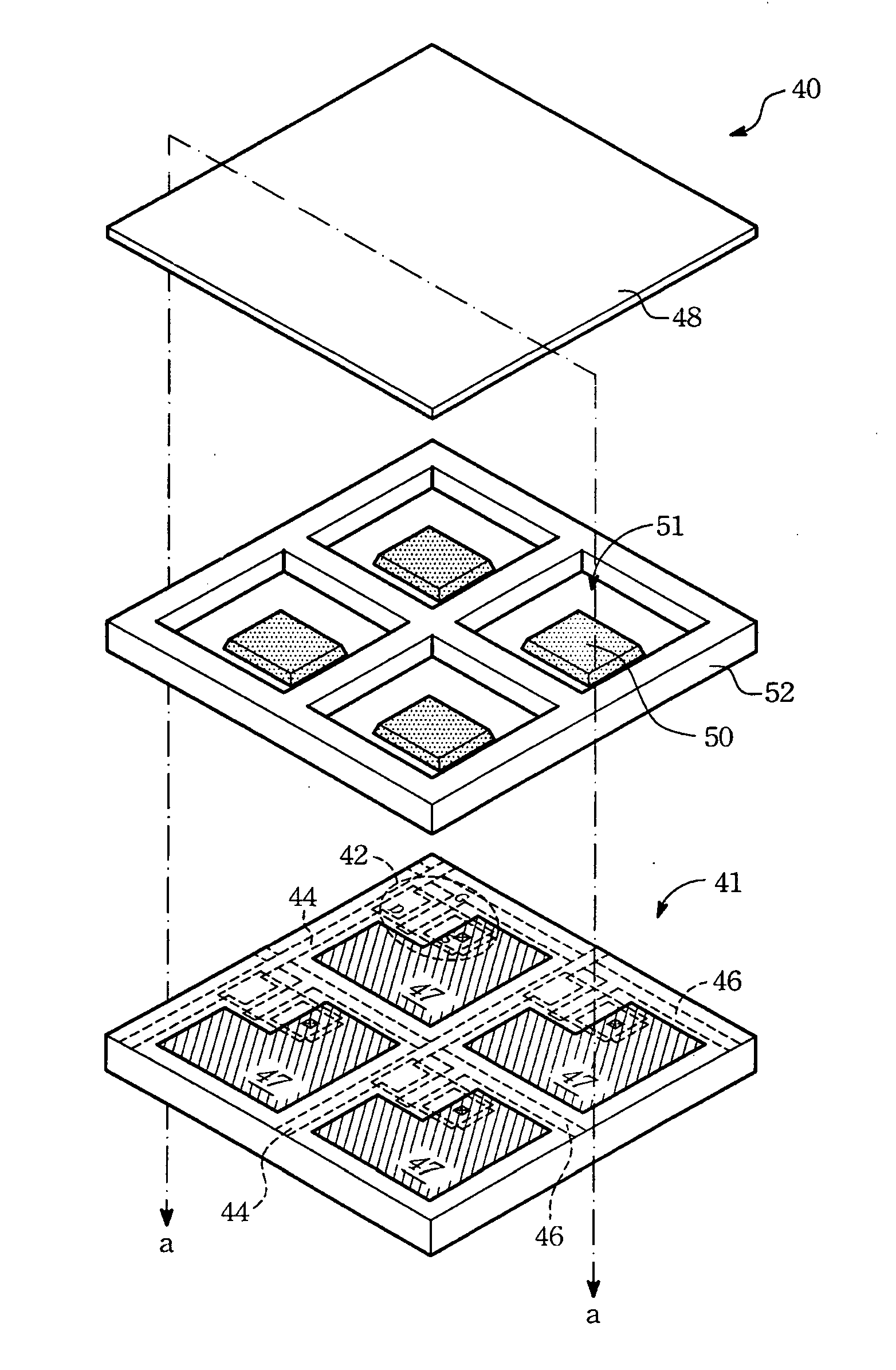
[0038] Referring to FIG. 3A and FIG. 3B. FIG. 3A shows an exploded view of a portion of a touch panel of the present invention. FIG. 3B is a cross-sectional view of the touch panel 40 shown in FIG. 3A along cross-sectional line a-a. FIG. 3A shows only four pieces of thin film transistors (TFTs) 42 for illustration. In the drawings, the thin film transistor 42 belongs to a bottom gate type, however, top gate typed thin film transistors can also be applied. The touch panel 40 can be applied to an electronic apparatus, ex. display panel, monitor, tablet computer, or like as. Any the display panel comprises liquid crystal display (LCD), organic light emitting display (OLED), polymer light emitting display (PLED), filed-emitting display (FED), plasmas display panel (PDP), surface-conduction electron-emitter display (SED), or like as. The touch panel 40 comprises a thin film transistor substrate 41, a plurality of conductive islets 47, a supporting pattern layer 52, and an elastic conduct...
PUM
 Abstract
Description
Claims
Application Information
 - R&D
- Intellectual Property
- Life Sciences
- Materials
- Tech Scout
- Unparalleled Data Quality
- Higher Quality Content
- 60% Fewer Hallucinations
Browse by: Latest US Patents, China's latest patents, Technical Efficacy Thesaurus, Application Domain, Technology Topic, Popular Technical Reports.
© 2025 PatSnap. All rights reserved.Legal|Privacy policy|Modern Slavery Act Transparency Statement|Sitemap|About US| Contact US: help@patsnap.com