
Thickness measuring device

Inactive Publication Date: 2006-07-13
HAMAMATSU PHOTONICS KK
View PDF4 Cites 0 Cited by
  • Summary
  • Abstract
  • Description
  • Claims
  • Application Information

AI Technical Summary

Benefits of technology

[0004] Therefore, an object of the invention is to provide a thickness measuring device which uses a Michelson interferometer, has a compact structure, and enables simple adjustment while enabling measurement with high accuracy.
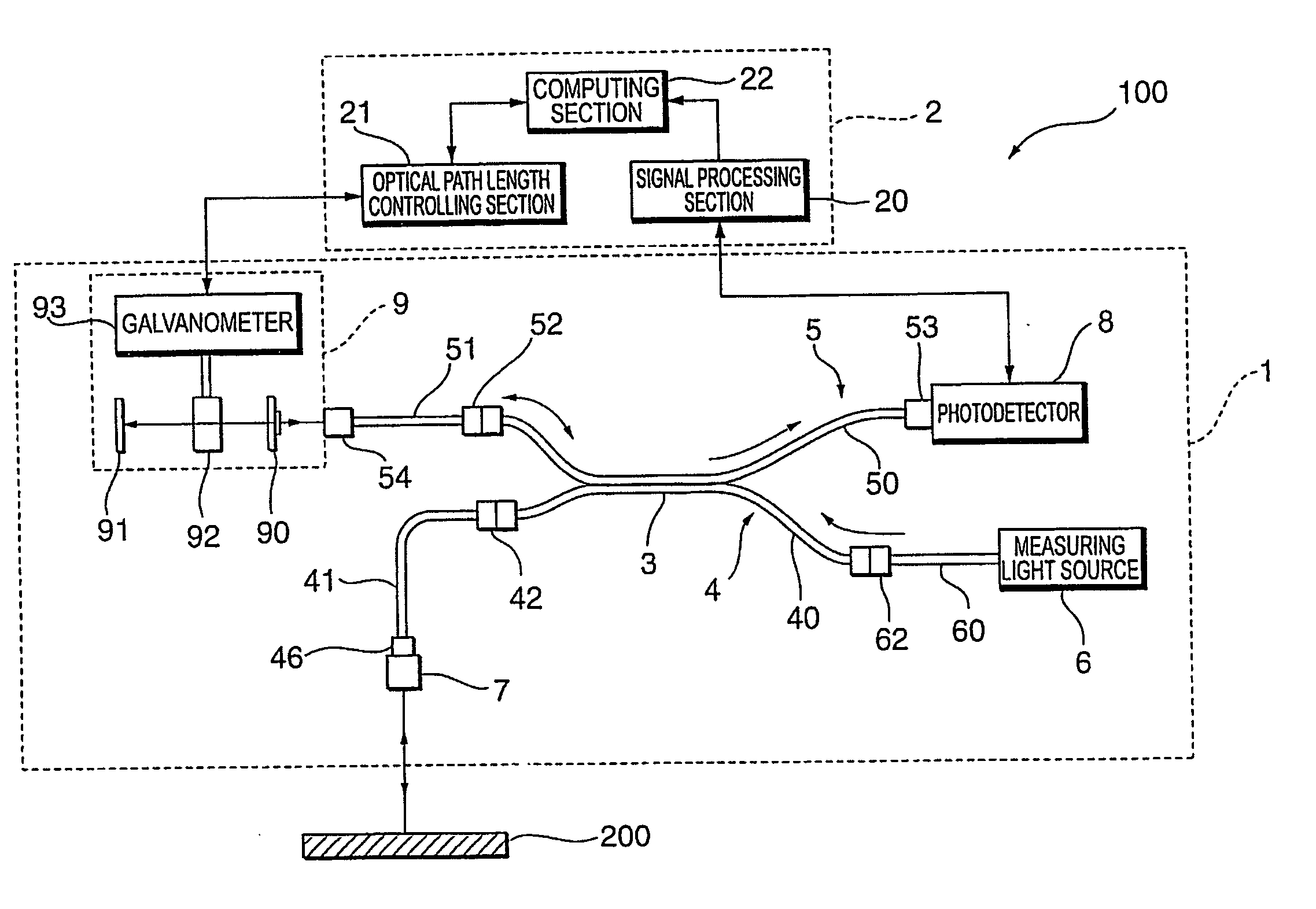
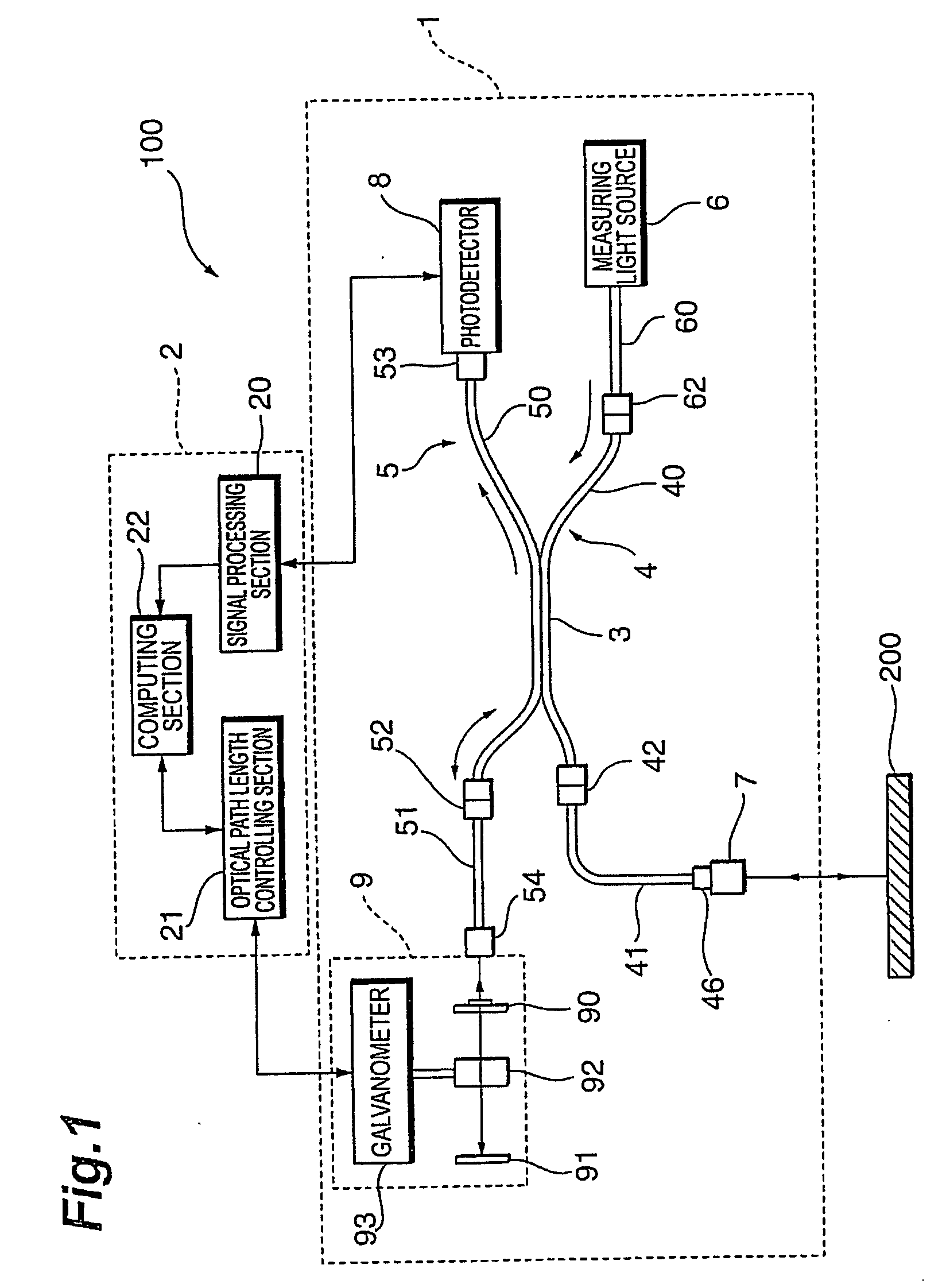
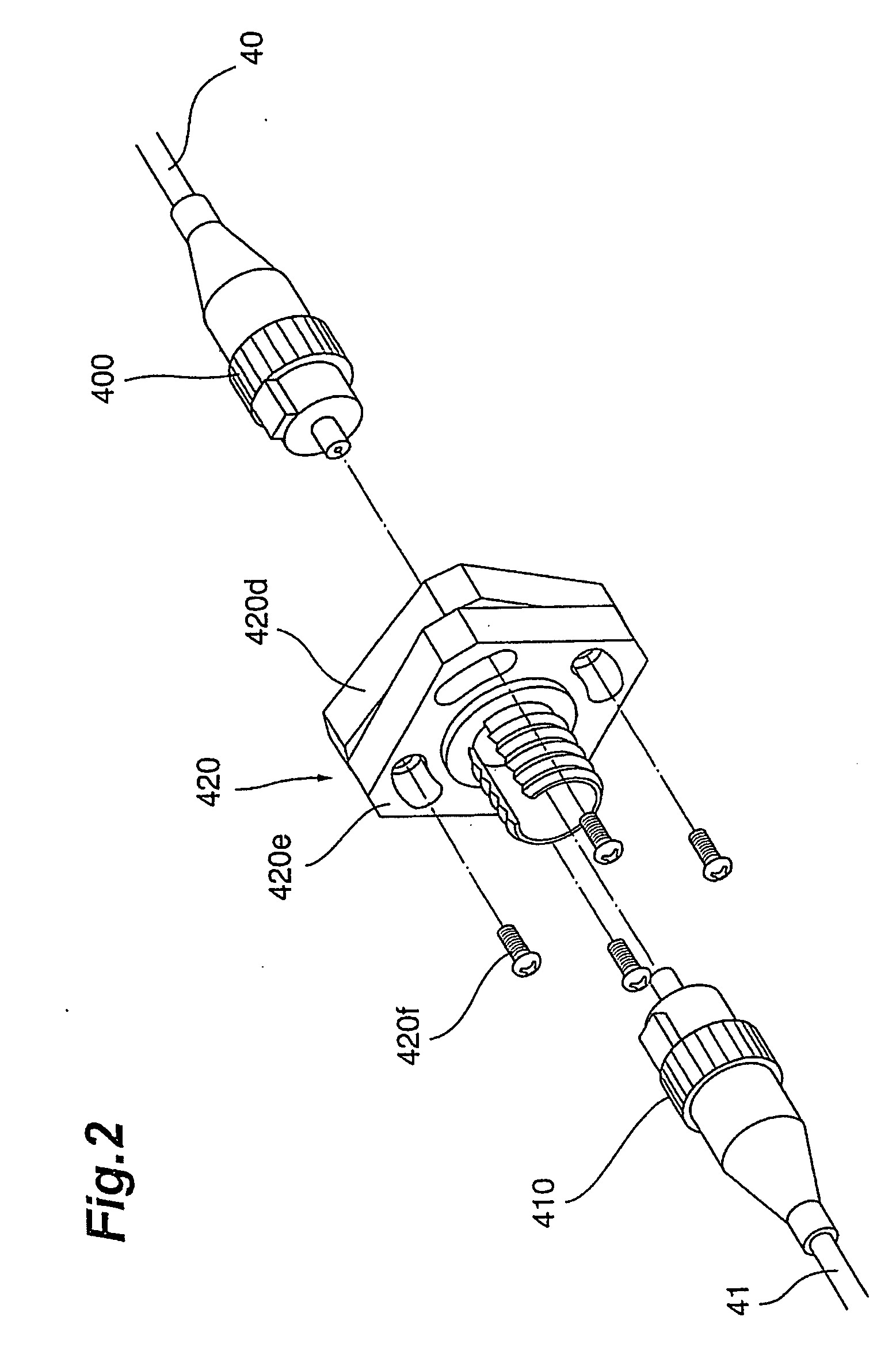
[0006] By forming the principle part of the optical system of the Michelson interferometer by optical fibers, the device becomes compact and the freedom of arrangement is increased. By using polarization-preserving optical fibers as the optical fibers, the plane of polarization is maintained even when the degree of bending the optical fibers is changed, so that stable generation of interference light becomes possible. Furthermore, connection of the polarization-preserving optical fibers by an optical connector makes it easy to manufacture and adjust the apparatus. Since this optical connector is structured so that the optical fibers to be connected can be rotated relatively, it can reliably match the direction of the plane of polarization between the optical fibers. Furthermore, by arranging a polarizer on the optical axis at least (1) between the optical coupler and the mirror in the reference optical system, (2) between the optical coupler and the light source, or (3) between the optical coupler and the object to be measured, noise components generated due to the rotation of the plane of polarization outside the optical coupler are cut and interference light signals can be detected with high accuracy.
[0007] It is preferable that at least one of the optical connectors has a polarizer disposed so as to rotate around the optical axis between the end faces of the optical fibers to be connected. By arranging a polarizer between the end faces of the optical fibers to be connected at the connector part, noise components are eliminated and measurement with high accuracy becomes possible.

Problems solved by technology

In order to increase the measuring accuracy in such a measuring device, it is required that an optical system in a Michelson interferometer 302 is accurately arranged, and this results in an increase in size of the apparatus or complicated adjustment of the system.

Method used


Image

  • Thickness measuring device
  • Thickness measuring device
  • Thickness measuring device

Examples


Embodiment Construction

[0017] Hereinafter, a preferred embodiment of the invention is described with reference to the accompanying drawings. To facilitate the comprehension of the explanation, the same reference numerals denote the same parts, where possible, throughout the drawings, and a repeated explanation will be omitted.

[0018]FIG. 1 is a schematic construction view showing an embodiment of the thickness measuring device according to the present invention. This thickness measuring device 100 is a Michelson interferometer type noncontact thickness meter which irradiates a semiconductor wafer 200 as a object to be measured with measuring light and uses a change in light intensity of interference light obtained by interference between reflected light from the semiconductor wafer 200 and reference light reflected by a reference optical system to measure the thickness of the semiconductor wafer 200.

[0019] This thickness measuring device 100 comprises a Michelson interferometer 1 and a calculation and co...


PUM


Abstract

A Michelson interferometer 1 of a thickness measuring device 100 comprises two optical cables 4 and 5 connected by an optical coupler 3, and the optical cables 4 and 5 are formed by polarization optical fibers 41 or the like, connected by the optical connectors 42 or the like. The optical connectors 42 or the like, are adjusted in angle and position by rotating the optical fibers 41 or the like, to be connected around the optical axis.

Description

TECHNICAL FIELD [0001] The present invention relates to a thickness measuring device for measuring the thickness of a semiconductor wafer, etc., more specifically, a thickness measuring device using a Michelson interferometer. BACKGROUND ART [0002] A thickness measuring device which uses a Michelson interferometer as a device for measuring the thickness of a semiconductor wafer, etc., in a noncontact manner is generally known. For example, in the apparatus disclosed in JP H10-325795A, as shown in FIG. 10, light emitted from a light source 301 is condensed by a condensing lens 303 and irradiated onto a object 308 to be measured, the object to be measured 308 or the condensing lens 303 and a reference light mirror 306 are moved, and the intensities of interference light on the front and back faces are measured by a photodetector 304, and from movement distances of the object 308 to be measured or the condensing lens 303 and the reference light mirror 306 when the intensity becomes max...

Claims


Application Information

Patent Timeline
IPC IPC(8): G01B11/02G01B9/02G01B11/06
CPCG01B11/06G01B11/0675G02B6/024G01B9/0209G01B2290/70
Inventor TAKAHASHI, TERUOSHIMIZU, TOHRU
Owner HAMAMATSU PHOTONICS KK
Learn More