

Thin film magnetic memory device reducing a charging time of a data line in a data read operation
a data read and data line technology, applied in semiconductor devices, digital storage, instruments, etc., can solve problems such as affecting the operation speed of data reading, and achieve the effect of reducing the charging time of data lines and bit lines, and fast data reading
- Summary
- Abstract
- Description
- Claims
- Application Information
AI Technical Summary
Benefits of technology
Problems solved by technology
Method used
Image

Examples
first embodiment
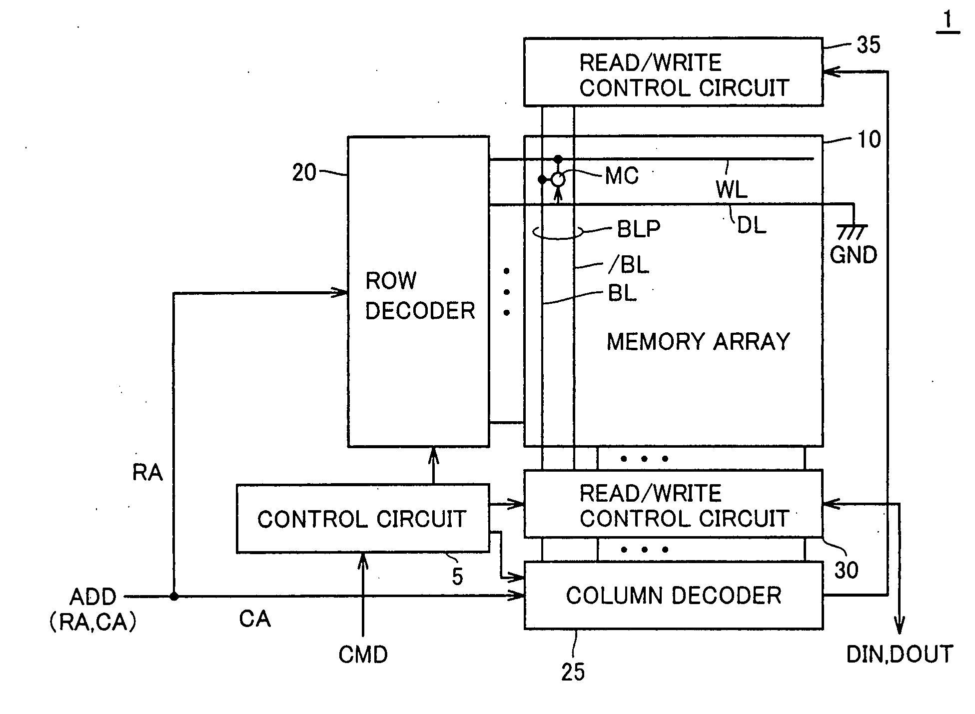
[0074] Referring to FIG. 1, an MRAM device 1 according to a first embodiment of the invention executes random access in response to a control signal CMD and an address signal ADD, which are externally applied, and executes input of write data DIN and output of read data DOUT.
[0075] MRAM device 1 includes a control circuit 5 for controlling a whole operation of MRAM device 1 in response to control signal CMD, and a memory array 10 having a plurality of MTJ memory cells MC arranged in rows and columns.
[0076] In memory array 10, a word line WL and a digit line DL are arranged corresponding to each row of the MTJ memory cells, and a bit line pair BLP formed of complementary bit lines BL and / BL is arranged corresponding to each column of the MTJ memory cells. FIG. 1 representatively shows one MTJ memory cell MC as well as an arrangement of word line WL, digit line DL and bit line pair BLP provided for MTJ memory cell MC.
[0077] MRAM device 1 further includes a row decoder 20, which de...
second embodiment
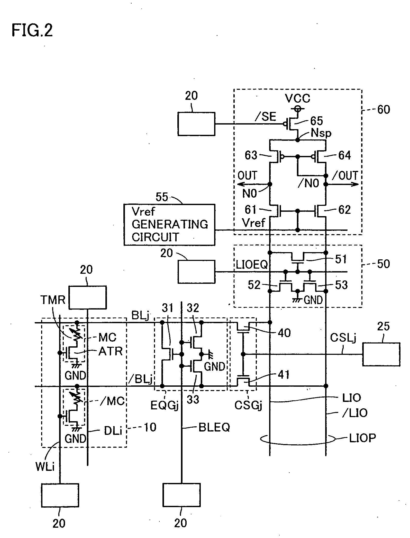
[0109] A second embodiment of the invention is aimed at suppression of an imbalance between capacitances of bit line pair BLP and data line pair LIOP, which may occur due to variations in respective elements during manufacturing.
[0110] Referring to FIG. 4, a structure of a data read circuit system according to a second embodiment differs from the structure shown in FIG. 2 in that a data line equalize circuit 50a is arranged in place of data line equalize circuit 50, and an equalize circuit EQGaj is arranged in place of equalize circuit EQGj.
[0111] Equalize circuit EQGaj differs from equalize circuit EQGj shown in FIG. 2 in that transistor switch 31 for equalizing is controlled independently of transistor switches 32 and 33 for precharging. More specifically, transistor switch 31 receives bit line equalize signal BLEQ on its gate, and transistors 32 and 33 both receive a bit line precharge signal BLPRE on their gates. Bit line precharge signal BLPRE is produced by row decoder 20.
[...
third embodiment
[0125] A third embodiment will now be described in connection with a structure, in which a predetermined voltage is used as a precharge voltage in stead of ground voltage GND.
[0126] Referring to FIG. 6, a structure of a data read circuit system according to the third embodiment differs from the structure shown in FIG. 2 in that a predetermined voltage VBL produced by a VBL generating circuit 54 is used as the precharge voltage to be supplied to equalize circuit EQGj instead of ground voltage GND. Further, predetermined voltage VBL is used as the precharge voltage to be supplied to data line equalize circuit 50 instead of ground voltage GND. Predetermined voltage VBL is set to a level corresponding to “Vref−Vth−Vmc” already described.
[0127] Referring to FIG. 7, description will now be given on the data read operation in the MRAM device according to the third embodiment. FIG. 7 representatively illustrates the operation to be performed when the ith row and the jth column are selecte...
PUM
 Abstract
Description
Claims
Application Information