Method and apparatus for constant bit rate data transmission in an optical burst switching network

a technology of optical burst switching and data transmission, applied in data switching networks, multiplex communication, digital transmission, etc., can solve the problems of delay in data transmission to different bit rate of data input into the optical burst switching network from that of data output therefrom, and increase the cost of the network. achieve the effect of efficiently transmitting user-defined data

Inactive Publication Date: 2006-07-20
SAMSUNG ELECTRONICS CO LTD
View PDF6 Cites 6 Cited by
  • Summary
  • Abstract
  • Description
  • Claims
  • Application Information

AI Technical Summary

Benefits of technology

[0017] Another aspect of the present invention is to provide a method for transmitting user desired data effic

Problems solved by technology

So, the electrical switch additionally needs an optoelectric converter to convert the optical signal into the electrical signal and electrooptic converter to convert the electrical signal into the optical signal, resulting in an increased cost.
However, a bit rate of data input into the optical burst switching network is different from

Method used


Image

  • Method and apparatus for constant bit rate data transmission in an optical burst switching network
  • Method and apparatus for constant bit rate data transmission in an optical burst switching network
  • Method and apparatus for constant bit rate data transmission in an optical burst switching network

Examples


Embodiment Construction

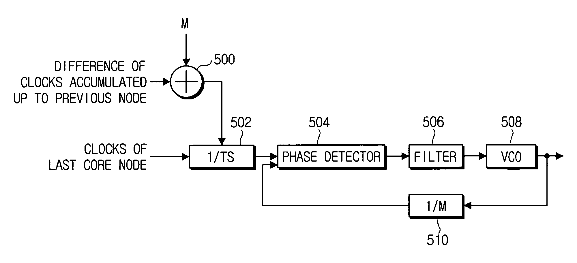
[0031] Hereinafter, a method for matching bit rates of data input to the optical burst switching network and of data output therefrom in accordance with an exemplary embodiment of the present invention will be described with reference to the accompanying drawings.

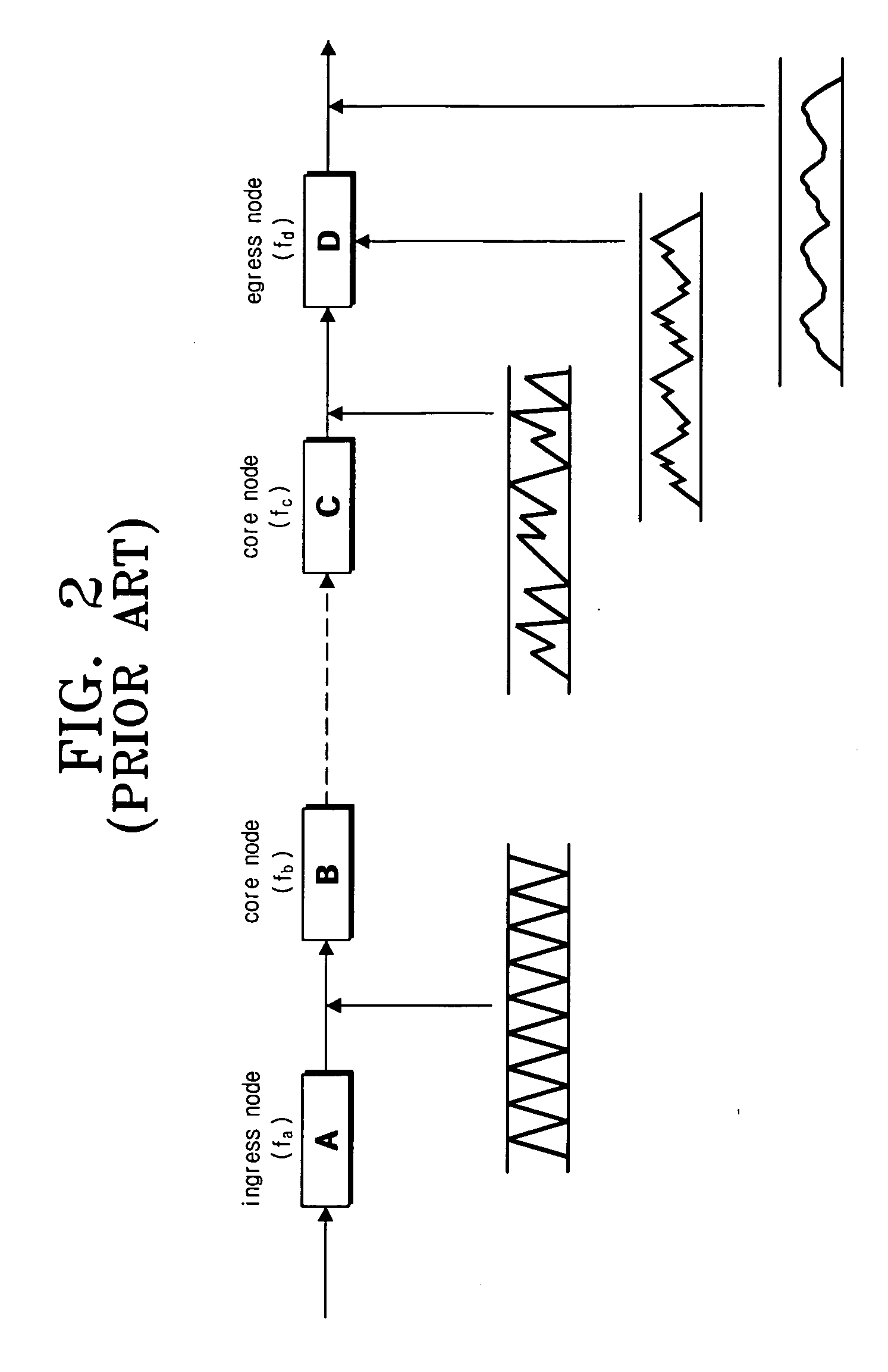
[0032]FIG. 3 shows an optical burst switching network constructed of an ingress edge node, an egress edge node, and a plurality of core nodes in accordance with an exemplary embodiment of the present invention. Hereinafter, operations performed in nodes constructing the optical burst switching network in accordance with an exemplary embodiment of the present invention will be described with reference to FIG. 3.

[0033] Referring to FIG. 3, each node processes data transferred in its natural frequency. That is, natural frequencies of node A, node B, node C and node D are fa, fb, fc and fd, respectively. Each node calculates a frequency difference between a frequency of data received on an input link of the node and the natur...


PUM


Abstract

A method, core node, ingress edge node, and egress edge node for matching a bit rate of data input into an optical burst switching network with that of data output from the optical burst switching network are provided. The method includes calculating a difference between a frequency of optical data received on a node and a natural frequency of the node; including the calculated difference into control information; and transmitting the control information. The core node includes a calculator to calculate a difference between frequency of optical data and the natural frequency of the optical data; and a controller to add the difference and a difference included in control information, and output the added difference. The ingress edge node includes a data processor; and a controller. The egress edge node includes an ingress edge node clock recovery phase lock loop; a de-mapper; and a storage unit.

Description

[0001] This application claims benefits under 35 U.S.C. § 119 from Korean Patent Application No. 2005-4691 filed on Jan. 18, 2005 and Korean Patent Application No. 2005-82802 filed on Sep. 6, 2005 in the Korean Intellectual Property Office. The entire contents of both applications are incorporated herein by reference. BACKGROUND OF THE INVENTION [0002] 1. Field of the Invention [0003] The present invention relates to an optical burst switching (OBS) network and, more specifically, to a method for matching a transmission rate of burst data input into an optical burst switching network and a transmission rate of burst data output. [0004] 2. Description of the Related Art [0005] Generally, when an optical signal is transmitted and received through an optical link, an electrical switch is used. However, the electrical switch must first convert the optical signal into an electrical signal, in order to process the optical signal transferred. Then, it must convert the processed electrical ...

Claims


Application Information

Patent Timeline
IPC IPC(8): H04J3/06
CPCH04B10/2507H04J3/0664H04Q11/0062H04Q2011/0079
Inventor DEN HOLLANDER, CORNELIS JOHANNISGARNER, GEOFFREY M.
Owner SAMSUNG ELECTRONICS CO LTD
Why Eureka
Try Eureka