

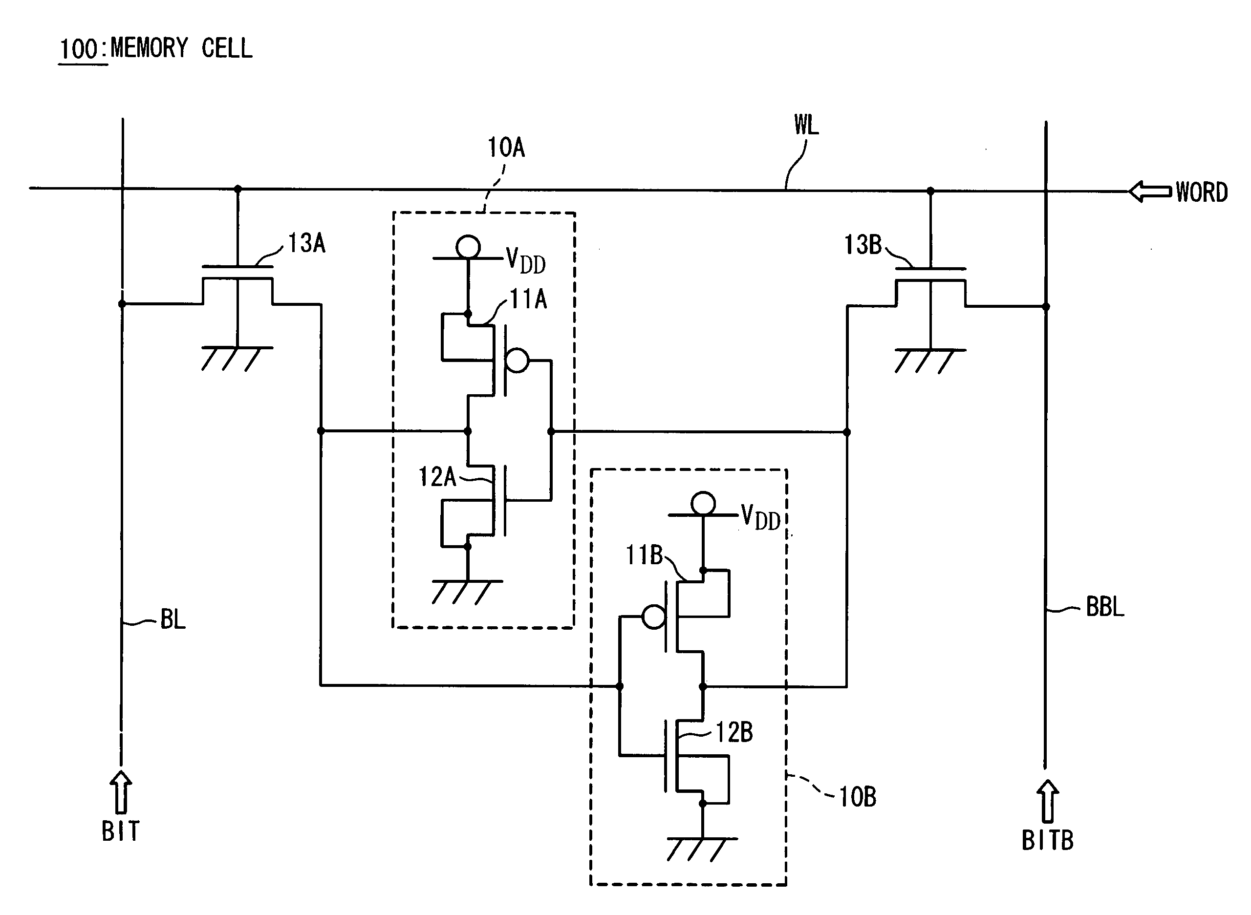
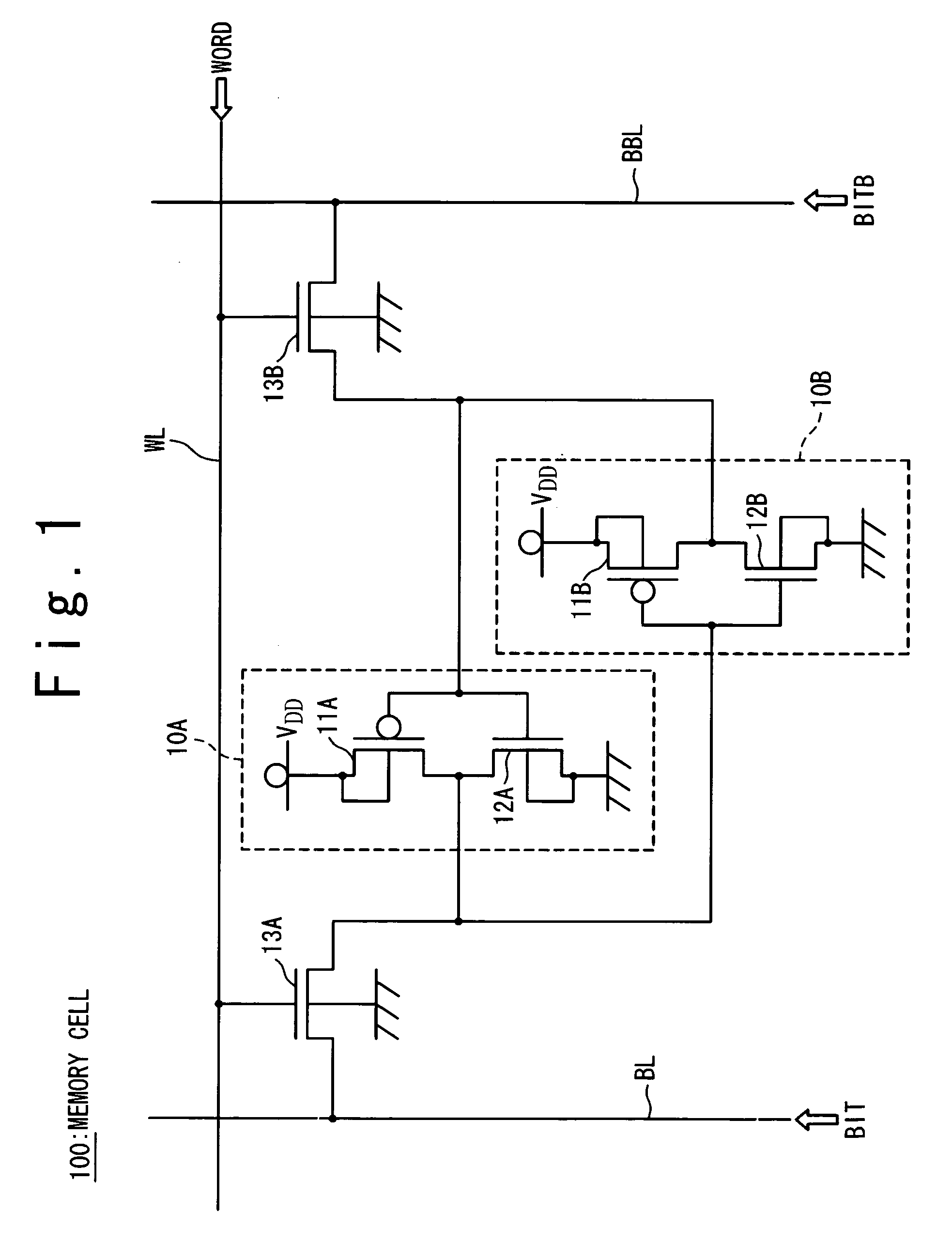
Static semiconductor memory device
a memory device and semiconductor technology, applied in semiconductor devices, digital storage, instruments, etc., can solve the problems of unexpected current flowing, leakage current flowing in normal dummy memory cells although slight, short circuit between, etc., to prevent leakage current flowing
- Summary
- Abstract
- Description
- Claims
- Application Information
AI Technical Summary
Problems solved by technology
Method used
Image

Examples
first embodiment
[0054] The SRAM according to the first embodiment of the present invention will be described with reference to FIGS. 3 to 11. In the SRAM in the first embodiment, dummy memory cells 201, 211 and 221 are used, in which the same P-type MOS transistor as the load transistor 11 in the memory cell 100 is used as a dummy load transistor.
[0055]FIG. 3 is a circuit diagram showing one of dummy memory cells 201 arranged in a direction of the bit lines in the SRAM according to the first embodiment of the present invention. The dummy memory cell 201 in the first embodiment is provided with dummy inverters 20-1 (20A-1 and 20B-1) corresponding to inverters 10 (10A and 10B) in the memory cell and dummy access transistors 23 (23A-1 and 23B-1) corresponding to the access transistors 13 (13A and 13B). Input and output terminals of the dummy inverters 20A-1 and 20B-1 are cross-connected to each other, and connected with the dummy access transistors 23A-1 and 23B-1. A source of the dummy access transi...
second embodiment
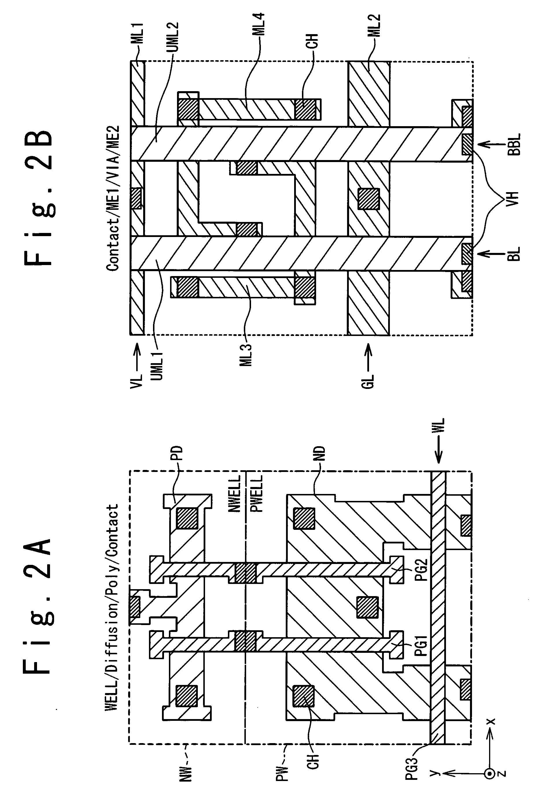
[0081] Next, the SRAM according to the second embodiment of the present invention will be described with reference to FIGS. 12A and 12B to 15A and 15B. When the P-type well PW region of the Tap cell 302 adjacent to the N-type well NW of the dummy memory cell 201 in the first embodiment can not be prepared due to miniaturization of the cell, the Tap cell 303 is used in the SRAM in the second embodiment in place of the Tap cell 302 in the SRAM in the first embodiment. In the Tap cell 303, the whole well layer WELL of the Tap cell is a P-type well PW. In addition, a dummy memory cell 202 is used in place of the dummy memory cell 201 in the first embodiment. The circuit configuration of the dummy memory cell 202 in the second embodiment is same as or similar to that of the dummy memory cell 201 shown in FIG. 3.
[0082]FIGS. 12A and 12B are diagrams showing layouts of the dummy memory cell 202. FIG. 12A shows the layout of the device section, and FIG. 12B shows the layout of the wiring se...
third embodiment
[0092] Next, the SRAM according to the third embodiment of the present invention will be described below with reference to FIGS. 16 to FIGS. 21A and 21B. The SRAM in the third embodiment includes the memory cells 100, each of which uses the load transistors 11 of a P-type MOS transistor, and the dummy memory cells, each of which dummy load transistors 21 of the N-type MOS transistor. FIG. 16 is a circuit diagram showing the dummy memory cell 203 used in the SRAM in the third embodiment. The dummy memory cell 203 in the third embodiment is provided with dummy inverters 20-2 (20A-2 and 20B-2) corresponding to the inverters 10 (10A and 10B) in the memory cell and dummy access transistors 23-2 (23A-2 and 23B-2) corresponding to the access transistors 13 (13A and 13B). The dummy inverters 20A-2 and 20A-2 are cross-connected to each other, and the gates of the dummy access transistors 23A-2 and 23B-2 are connected to the word line WL.
[0093] Referring to FIG. 16, the dummy inverters 20-2 ...
PUM
 Abstract
Description
Claims
Application Information