Method for producing solid-state imaging device, solid-state imaging device, and camera

Active Publication Date: 2006-07-27
SONY SEMICON SOLUTIONS CORP
View PDF10 Cites 11 Cited by
  • Summary
  • Abstract
  • Description
  • Claims
  • Application Information

AI Technical Summary

Benefits of technology

[0030] According to the method for producing the solid-state imaging device of the embodiment of the present invention, it is able to produce the solid-state imaging device in which the light sensitivity chara

Problems solved by technology

However, in the above method for producing the solid-state ima

Method used


Image

  • Method for producing solid-state imaging device, solid-state imaging device, and camera
  • Method for producing solid-state imaging device, solid-state imaging device, and camera
  • Method for producing solid-state imaging device, solid-state imaging device, and camera

Examples


Embodiment Construction

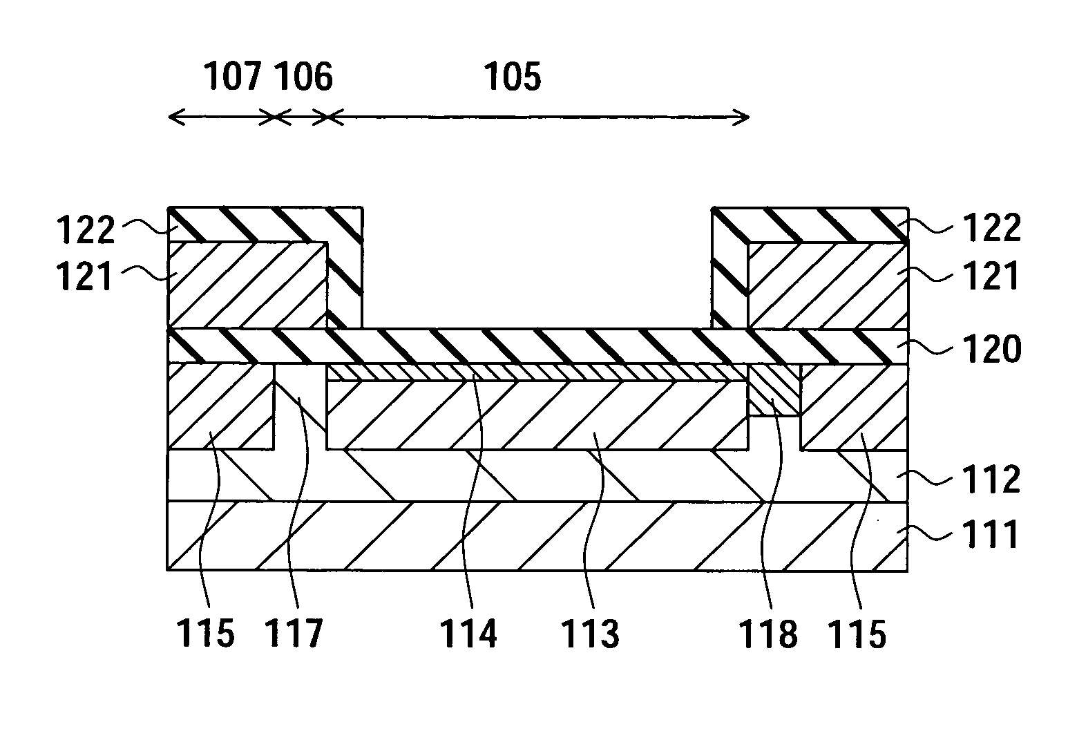
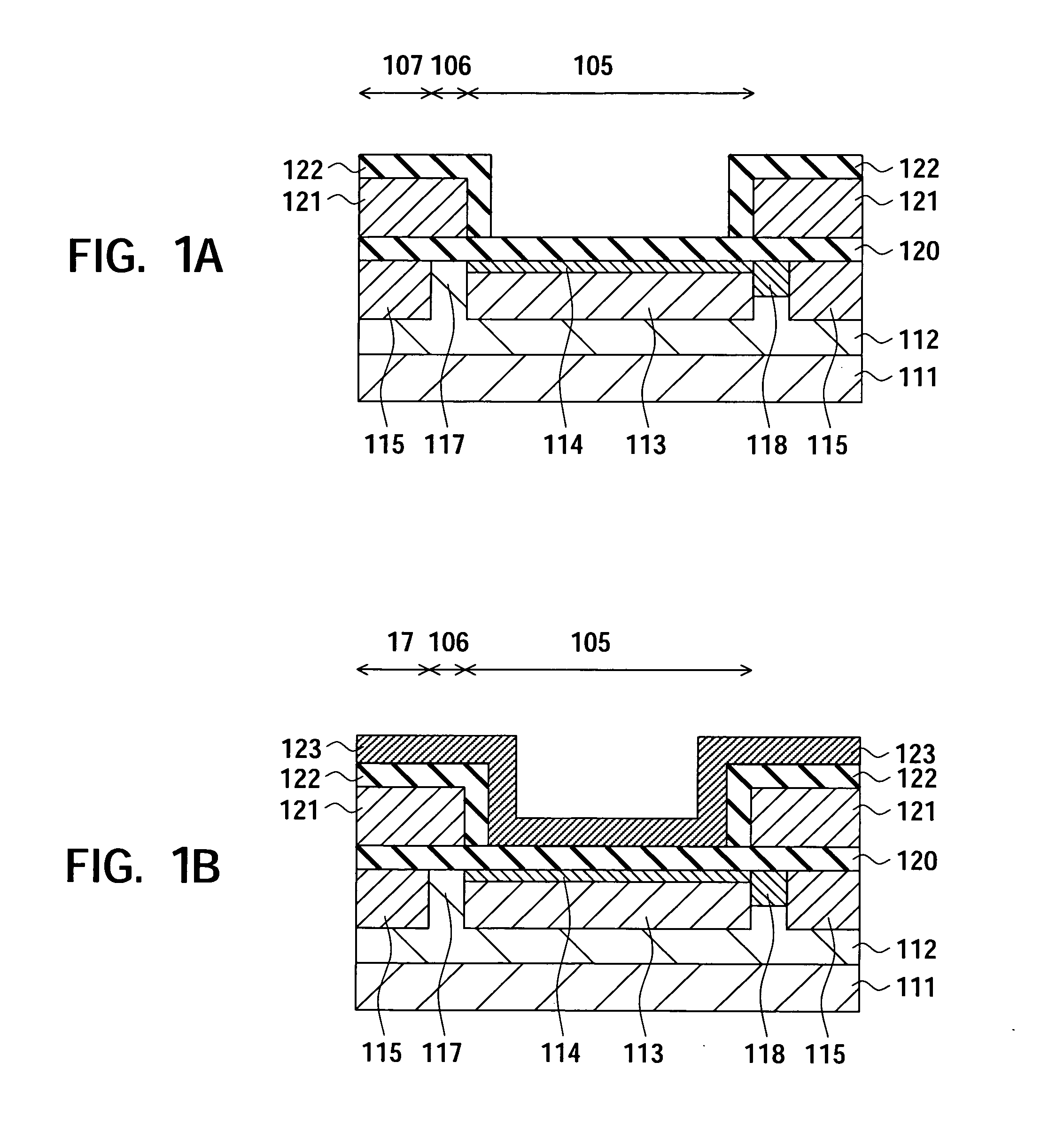
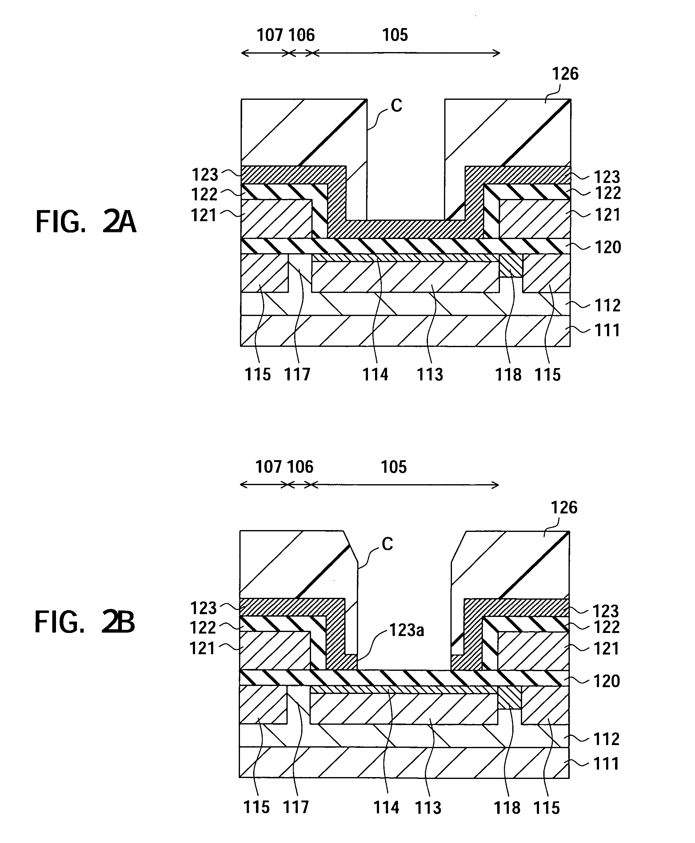
[0052] Preferred embodiments of the present invention will be described in more detail with reference to the accompanying drawings. In the present embodiment, an example applying the present invention to an interline transfer type solid-state imaging device will be described.

[0053]FIG. 6 is a schematic configuration view of a solid-state imaging device according the present embodiment.

[0054] A solid-state imaging device 1 according to the present embodiment is provided with an imaging region 2, a horizontal transfer unit 3 and an output unit 4.

[0055] The imaging region 2 has a plurality of light receiving units 5 arranged in matrix, a plurality of vertical transfer units 7 arranged in every row of the light receiving units 5, and read out gate units 6 placed between the light receiving unit 5 and the vertical transfer unit 7.

[0056] The light receiving unit 5 is formed by a photo diode, for example, converts an imaging light (incidence light) emitted from an object to be imaged t...


PUM


Abstract

To provide a method for producing a solid-state imaging device enabling an improvement of a light sensitivity characteristic in a light receiving unit, a solid-state imaging device in which the light sensitivity characteristic is improved, and a camera provided with the solid-state imaging device. A shield film projected around the light receiving unit is formed on a substrate in which the light receiving unit is formed; an transparent insulation film is formed on the shield film; a sidewall insulation film is formed by etch-back of the insulation film, in a side wall of the shield film; a mask layer having an aperture at a position corresponding to the light receiving unit is formed on the shield film; and the shield film is etched by using the sidewall insulation film and the mask layer as a mask to form an aperture portion exposing the light receiving unit.

Description

CROSS REFERENCES TO RELATED APPLICATIONS [0001] The present invention contains subject matter related to Japanese Patent Application No. JP 2005-19796 filed in the Japanese Patent Office on Jan. 27, 2005, the entire contents of which being incorporated herein by reference.BACKGROUND OF THE INVENTION [0002] 1. Field of the Invention [0003] The present invention relates to a method for producing a solid-state imaging device, a solid-state imaging device, and a camera, for example, a method for producing a solid-state imaging device such as a charge coupled device (CCD), the solid-state imaging device, and a camera provided with the solid-state imaging device. [0004] 2. Description of the Related Art [0005] A method for producing a solid-state imaging device in related art will be described with reference to FIGS. 1A and 1B, FIGS. 2A and 2B, and FIGS. 3A and 3B. [0006] As shown in FIG. 1A, an n-type signal charge storage region 113, an n-type transfer channel region 115, and a channel ...

Claims


Application Information

Patent Timeline
IPC IPC(8): H01L21/00H01L27/14H04N5/335H04N5/369H04N5/372
CPCH01L27/1462H01L27/14621H01L27/14627H01L27/14683H01L27/14685H01L27/14818H01L27/14837H01L27/148
Inventor MIYAMOTO, HIROYUKIDOFUKU, TADAYUKI
Owner SONY SEMICON SOLUTIONS CORP
Why Eureka
Try Eureka