Photodetector, liquid crystal display device, and light emitting device

Inactive Publication Date: 2011-02-24
SEMICON ENERGY LAB CO LTD
View PDF32 Cites 31 Cited by
  • Summary
  • Abstract
  • Description
  • Claims
  • Application Information

AI Technical Summary

Benefits of technology

[0020]The light-blocking layer between the first photodiode and the second photodiode allows the light from an obj

Problems solved by technology

However, it is difficult to prevent light from a backlight from entering photoelectric

Method used


Image

  • Photodetector, liquid crystal display device, and light emitting device
  • Photodetector, liquid crystal display device, and light emitting device
  • Photodetector, liquid crystal display device, and light emitting device

Examples


embodiment 1

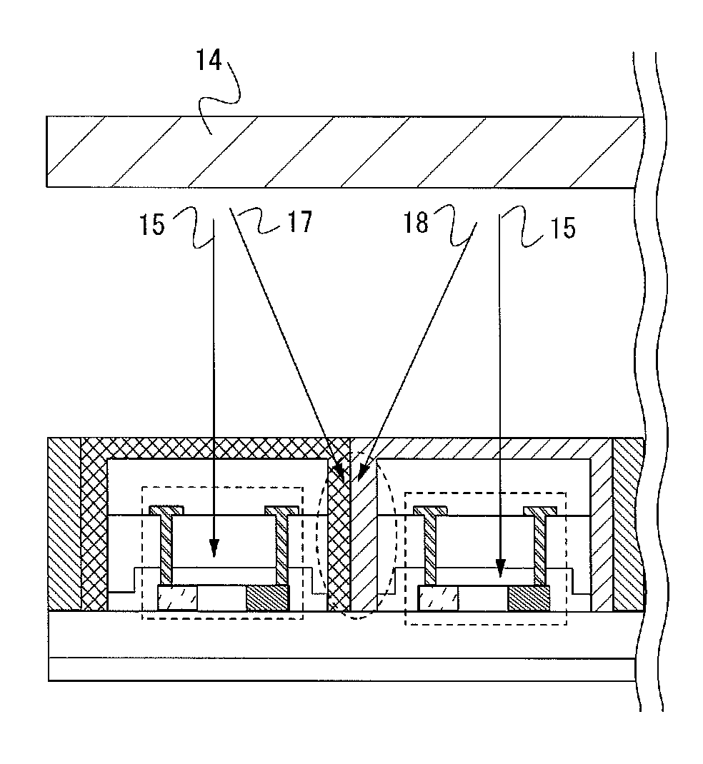
[0036]A photodetector which is one embodiment of the present invention will be described (FIG. 1). FIG. 1 is a cross-sectional view of the photodetector.

[0037]The photodetector which is one embodiment of the present invention includes a first light-blocking layer 2 and a second light-blocking layer 3 over a light-transmitting substrate 1, a first photodiode 4 over the first light-blocking layer, a second photodiode 5 over the second light-blocking layer 3, a first color filter 6 covering the first photodiode 4, and a second color filter 7 covering the second photodiode 5. The photodetector includes a third light-blocking layer 8 formed using the first color filter 6 and the second color filter 7 and disposed between the first photodiode 4 and the second photodiode 5.

[0038]The third light-blocking layer 8 is formed using the first color filter 6 and the second color filter 7 which are arranged side by side. In other words, the third light-blocking layer 8 is formed using one end of t...

embodiment 2

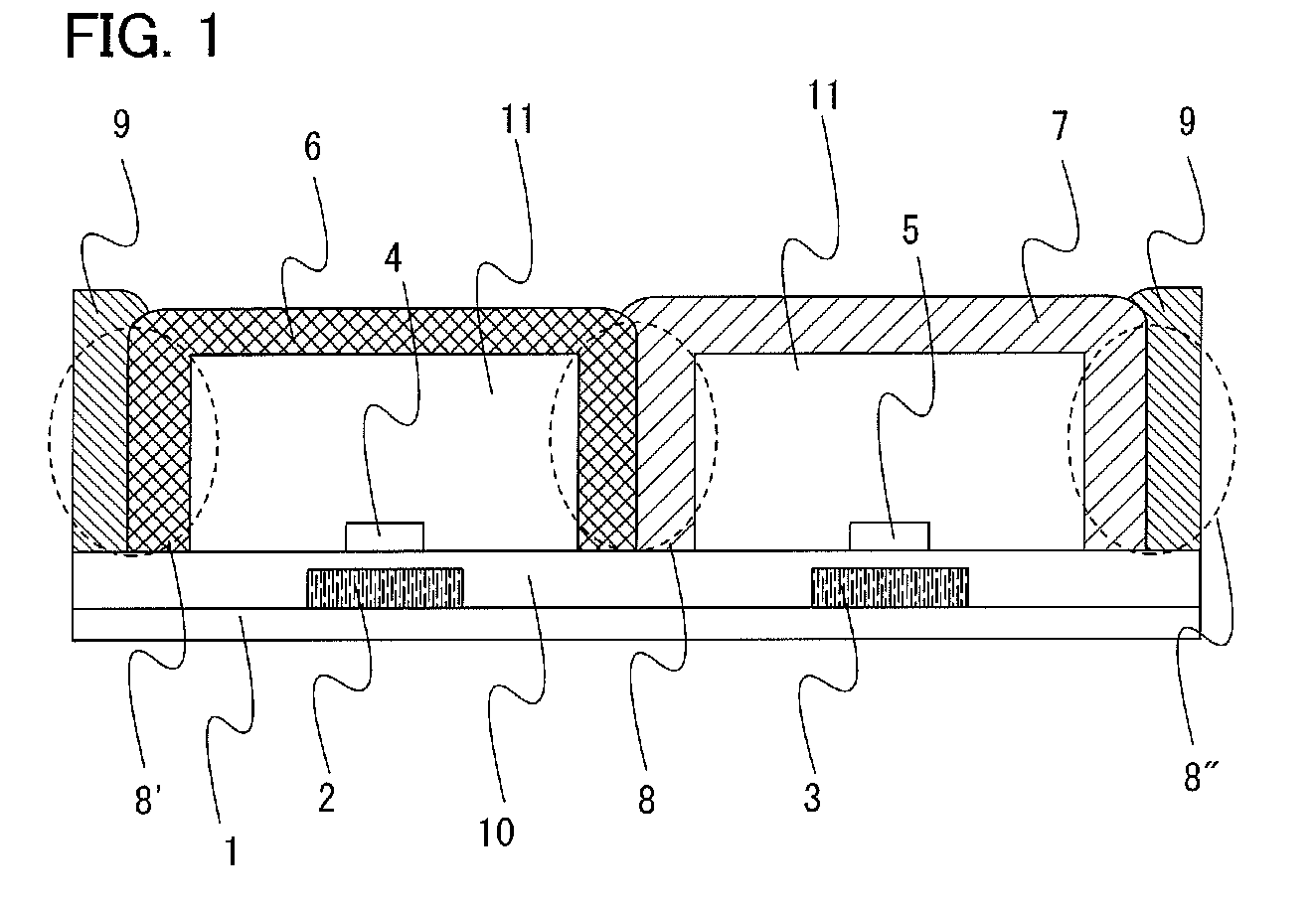
[0065]A liquid crystal display device which is one embodiment of the present invention will be described (FIG. 6). FIG. 6 is a cross-sectional view of the liquid crystal display device.

[0066]The liquid crystal display device which is one embodiment of the present invention includes the first light-blocking layer 2 and the second light-blocking layer 3 which are over the first light-transmitting substrate 1, the first photodiode 4 over the first light-blocking layer 2, the second photodiode 5 over the second light-blocking layer 3, the first color filter 6 covering the first photodiode 4, and the second color filter 7 covering the second photodiode 5. The liquid crystal display device includes the third light-blocking layer 8 formed using the first color filter 6 and the second color filter 7, between the first photodiode 4 and the second photodiode 5. Further, the liquid crystal display device includes a liquid crystal layer 53 over the first color filter 6 and the second color filt...

embodiment 3

[0119]A light-emitting device which is one embodiment of the present invention will be described below (FIG. 10). FIG. 10 is a cross-sectional view of the light-emitting device. The liquid crystal display device in Embodiment 2 and the light-emitting device in Embodiment 3 are different in that the liquid crystal display device in Embodiment 2 includes the liquid crystal layer, the first light-blocking layer 2, the second light-blocking layer 3, and the light-blocking layer 31, while the light-emitting device in Embodiment 3 includes an electroluminescent (EL) layer and hence does not need to include the first light-blocking layer 2, the second light-blocking layer 3, and the light-blocking layer 31. The display device in the Embodiment 2 and the light-emitting device in Embodiment 3 are also different in the method of detecting light: the display device in the Embodiment 2 uses the backlight, while the light-emitting device in Embodiment 3 uses an EL layer instead of a backlight.

[0...


PUM


Abstract

One embodiment of the present invention includes a first light-blocking layer and a second light-blocking layer which are over a light-transmitting substrate, a first photodiode over the first light-blocking layer, a second photodiode over the second light-blocking layer, a first color filter covering the first photodiode, a second color filter covering the second photodiode, and a third light-blocking layer formed using the first color filter and the second color filter and disposed between the first photodiode and the second photodiode.

Description

BACKGROUND OF THE INVENTION[0001]1. Field of the Invention[0002]The present invention relates to a photodetector including a photodiode, a liquid crystal display device including a photodiode, and a light-emitting device including a photodiode.[0003]2. Description of the Related Art[0004]Patent Document 1 discloses a liquid crystal display device having an input function using a photosensor. Specifically, the liquid crystal display device includes a switching element and a photoelectric conversion element over a light-transmitting substrate. The thickness of the light-transmitting substrate is 70 to 100 μm. The light-transmitting substrate having such a thickness prevents stray light from a backlight from entering the photoelectric conversion element.REFERENCE[0005][Patent Document 1] Japanese Published Patent Application No. 2005-10690SUMMARY OF THE INVENTION[0006]However, it is difficult to prevent light from a backlight from entering photoelectric conversion element (a photodiode...

Claims


Application Information

Patent Timeline
IPC IPC(8): H01L31/0232H01L31/12G02F1/1335
CPCG02F1/133514G02F2001/13312H01L27/1446H01L31/02327H01L27/14621H01L31/02164H01L27/14618H01L2924/0002G02F1/13312H10K59/13H01L2924/00H01L27/14643
Inventor KUROKAWA, YOSHIYUKIIKEDA, TAKAYUKI
Owner SEMICON ENERGY LAB CO LTD
Why Eureka
Try Eureka