Image display device

a display device and flat panel technology, applied in the direction of discharge tube/lamp details, discharge tube/lamp details, cathode ray tube/electron beam tube, etc., can solve the problems of metal back film thickness reduction, electrical conductivity and light reflectance reduction, and metal back film peeling, etc., to improve white brightness, small differences in light reflectance of aluminum, and high brightness

Inactive Publication Date: 2006-08-03
HITACHI DISPLAYS
View PDF7 Cites 20 Cited by
  • Summary
  • Abstract
  • Description
  • Claims
  • Application Information

AI Technical Summary

Benefits of technology

[0013] An anode voltage of FPD of the electron emission type is generally selected to be in a range of from several kilovolts to some dozen kilovolts, and therefore the anode voltage of the FPD of the electron emission type is lower than 25-30 kV required for driving of cathode ray tubes. Electron beams emitted from the electro sources lose their energy due to the presence of an electro-conductive light-reflective film (hereinafter a metal back or a metal back film) which covers phosphor layers and serves as the anode, and consequently, brightness of the image display device is greatly degraded. Therefore it is indispensable to make the metal back film thinner for eliminating this problem.

Problems solved by technology

However, reducing of the thickness of the metal back film produces side effects of reductions in electrical conductivity and light reflectance, and it is necessary to select the thickness and density of the metal back film so as to strike a balance among the reductions in display brightness, electrical conductivity and light reflectance.
In the case of cathode ray tubes, the metal back film can be considered as located in a space where no electric fields are present, but in the case of the FPD of the electron emission type, since the spacing between the front and rear substrates are selected in a range of from several millimeters to several tens of millimeters, the metal back film are located under strong electric fields of 2 kV / mm to 3 kV / mm, are always subjected to strong coulomb forces during operation of the FPD of the electron emission type, and there is a fear of peeling of the metal back film.
However, there are problems in that in the case of the dense and continuous metal back film it is difficult to form pinholes therein and the film itself swells and breaks easily, and this problems need to be solved.

Method used


Image

  • Image display device
  • Image display device
  • Image display device

Examples


embodiment 1

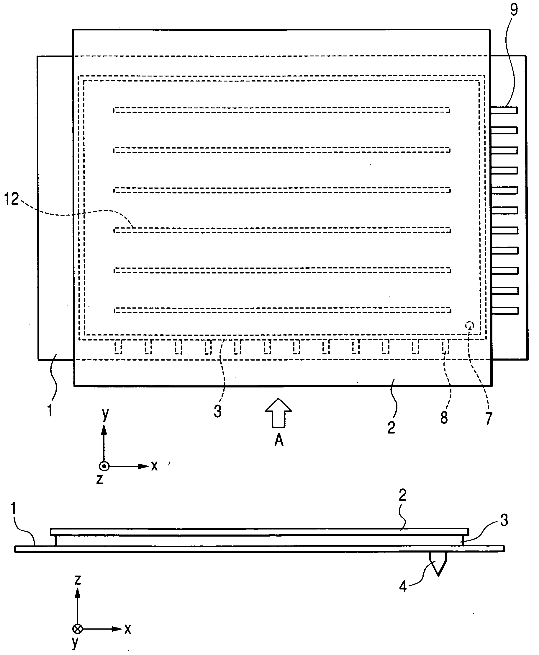
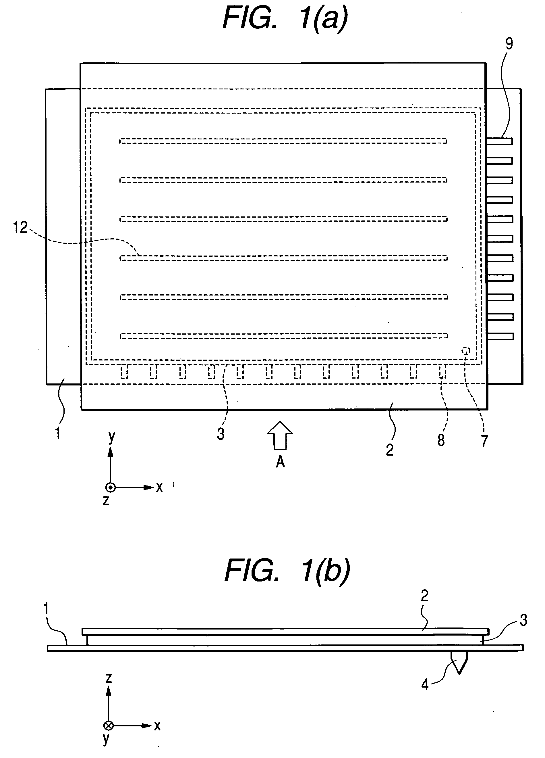
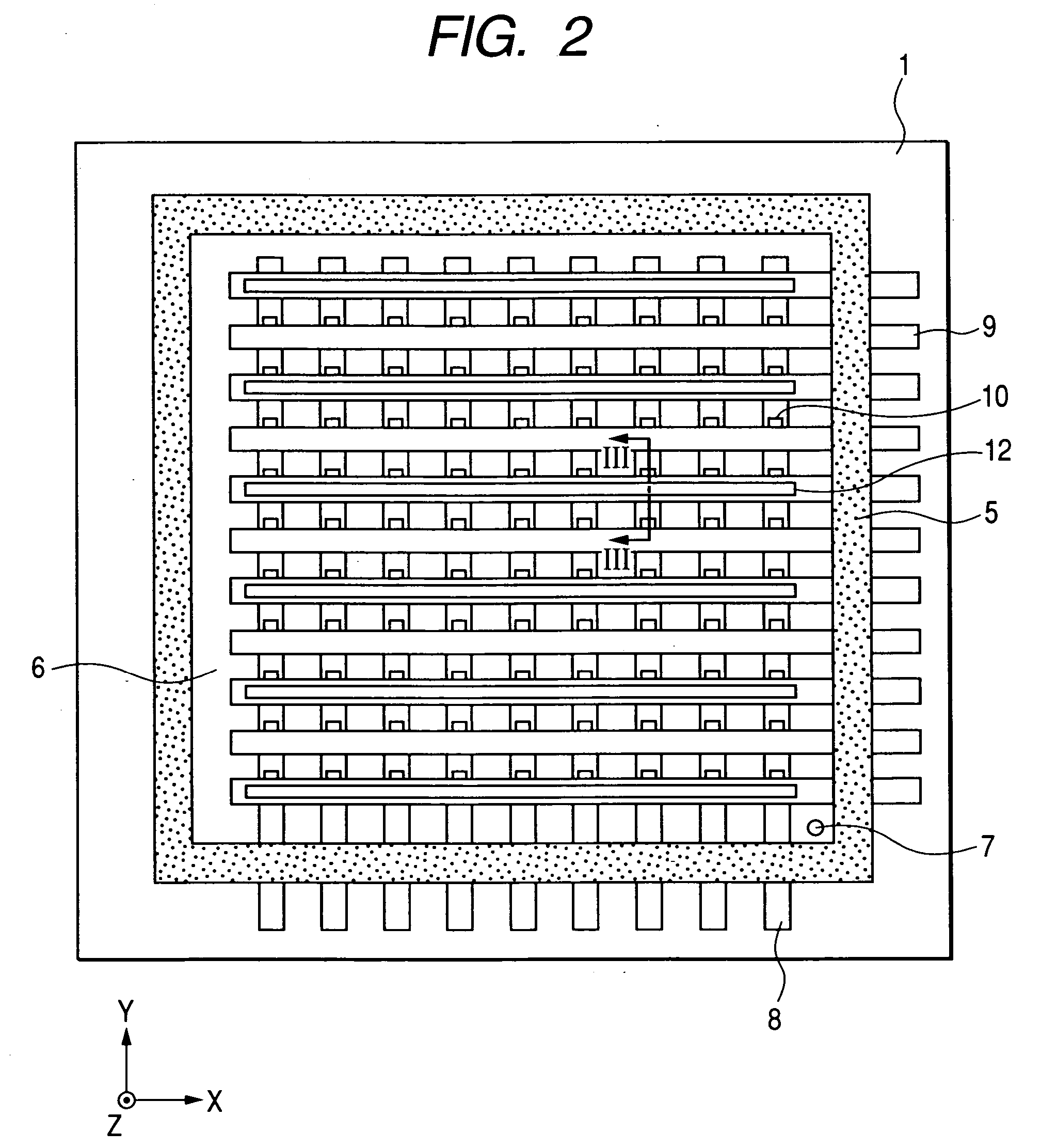
[0066]FIG. 1 (a) to FIG. 3 illustrate an embodiment of the image display device in accordance with the present invention. FIG. 1(a) is a plan view of the image display device viewed from its front-substrate side, FIG. 1(b) is a side view of the image display device viewed in a direction of an arrow A in FIG. 1(a), FIG. 2 is a schematic plan view of a rear substrate of the image display device of FIG. 1 with its front substrate removed, and FIG. 3 is a schematic cross-sectional view of the rear substrate of FIG. 2 taken along line III-III of FIG. 2 and a corresponding portion of the front substrate taken along line III-III. In FIGS. 1(a) to 3, reference numerals 1 and 2 denote the rear and front substrates, respectively, which are made of glass plates of several millimeters, for example about 3 mm, in thickness. Reference numeral 3 denotes a support member, which is made of a glass plate or a sintered glass frit of several millimeters, for example about 3 mm, in thickness. Reference ...

embodiment 2

[0091]FIG. 7 shows another embodiment of the image display device in accordance with the present invention, and is a schematic plan view of a phosphor screen of the image display device viewed from the outside of the front substrate. The same reference numerals as utilized in the previous figures designate corresponding portions in FIG. 7.

[0092] In FIG. 7, a BM film 16 is formed in a portion corresponding to the display area 6 on the front substrate 2, and the BM film 16 is provided with plural openings (windows) 161 in the form of parallel lines. Green phosphor layers 15G, blue phosphor layers 15B and red phosphor layers 15R are deposited to fill corresponding ones of the openings 161. In this configuration, the phosphor layers 15 extend a distance of the width Wx across the width Ww of the opening 161 in the X direction, and extend a distance of the entire length of the display area 6 in the Y direction, and the BM film 16 extends a distance of the width Wb in the X direction and...

embodiment 3

[0097]FIG. 8 is a process chart for explaining a method of fabricating an image display device in accordance with the present invention. The same reference numerals as utilized in FIG. 1(a) to FIG. 7 designate corresponding portions in FIG. 7.

[0098] In FIG. 8, the front substrate 2 includes on a glass substrate a phosphor screen comprised of the BM film 16, the phosphor pattern 15 and the metal back film (anode) 17. A preliminary front-substrate assembly FTA is obtained by coating a sealing member 5 comprised of noncrystalline glass frit kneaded with appropriate binder and adhesive members 13 for fixing spacers 7 and comprised of glass frit, for example, kneaded with appropriate binder, in the respective desired patterns on the front substrate 2 of the above configuration.

[0099] Here, instead of forming the sealing member 5 on the substrates, all of the sealing members may be formed on the support member 3.

[0100] After subjecting the preliminary front-substrate assembly FTA to a ...


PUM


Abstract

An image display device includes: a front substrate having phosphor layers and a light reflective film succeeding the phosphor layers and composed chiefly of aluminum on an inner surface thereof; a rear substrate having plural electron sources on an inner surface thereof, and disposed to oppose the front substrate with a specified spacing between the front and rear substrates; and a support member which is sandwiched between the front and rear substrates, surrounds a display area formed between the front and rear substrates, and maintains the specified spacing. Two end faces of the support member are hermetically sealed to the front substrate and the rear substrate, respectively, via sealing members. A thickness of the light reflective film is in a range of from 50 nm to 200 nm, and an average film density of the light reflective film is in a range of from 1.6 g / cm3 to 2.6 g / cm3.

Description

CLAIM OF PRIORITY [0001] The present application claims priority from Japanese application serial No. 2005-010414, filed on Jan. 18, 2005, the content of which is hereby incorporated by reference into this application. BACKGROUND OF THE INVENTION [0002] The present invention relates to a flat panel type image display device which utilizes emission of electrons into a vacuum produced between a front substrate and a rear substrate, and in particular to an image display device provided with a light-reflective film disposed to cover phosphors on the front substrate. [0003] Conventionally, color cathode ray tubes have been widely used as display devices excellent in producing high-brightness high-definition display devices. However, as the image quality in information processing equipment and TV broadcasts has been improved in recent years, the demand has been becoming stronger for flat panel type display devices (hereinafter FPD) capable of realizing lighter weight and space-saving in a...

Claims


Application Information

Patent Timeline
Patent Type & Authority Applications(United States)
IPC IPC(8): H01J63/04
CPCH01J31/127
Inventor TOJO, TOSHIOHAYASHI, NOBUYASUTAKAHASHI, KATSUYUU
Owner HITACHI DISPLAYS
Why Eureka
Try Eureka