Low noise amplifier for ultra wide band

Active Publication Date: 2006-08-03
SAMSUNG ELECTRONICS CO LTD
View PDF8 Cites 28 Cited by
  • Summary
  • Abstract
  • Description
  • Claims
  • Application Information

AI Technical Summary

Benefits of technology

[0021] The low noise amplifier may further include a buffer amplifying element which may includ

Problems solved by technology

A radio frequency (RF) signal, which is a high frequency signal received via an antenna, has a very low power level due to attenuation and nois

Method used


Image

  • Low noise amplifier for ultra wide band
  • Low noise amplifier for ultra wide band
  • Low noise amplifier for ultra wide band

Examples


Example

[0029] Certain exemplary embodiments of the present invention will now be described in greater detail with reference to the accompanying drawings.

[0030] In the following description, same drawing reference numerals are used for the same elements even in different drawings. The matters defined in the description, such as detailed construction and element descriptions, are provided to assist in a comprehensive understanding of the invention. Also, well-known functions or constructions are not described in detail since they would obscure the invention in unnecessary detail.

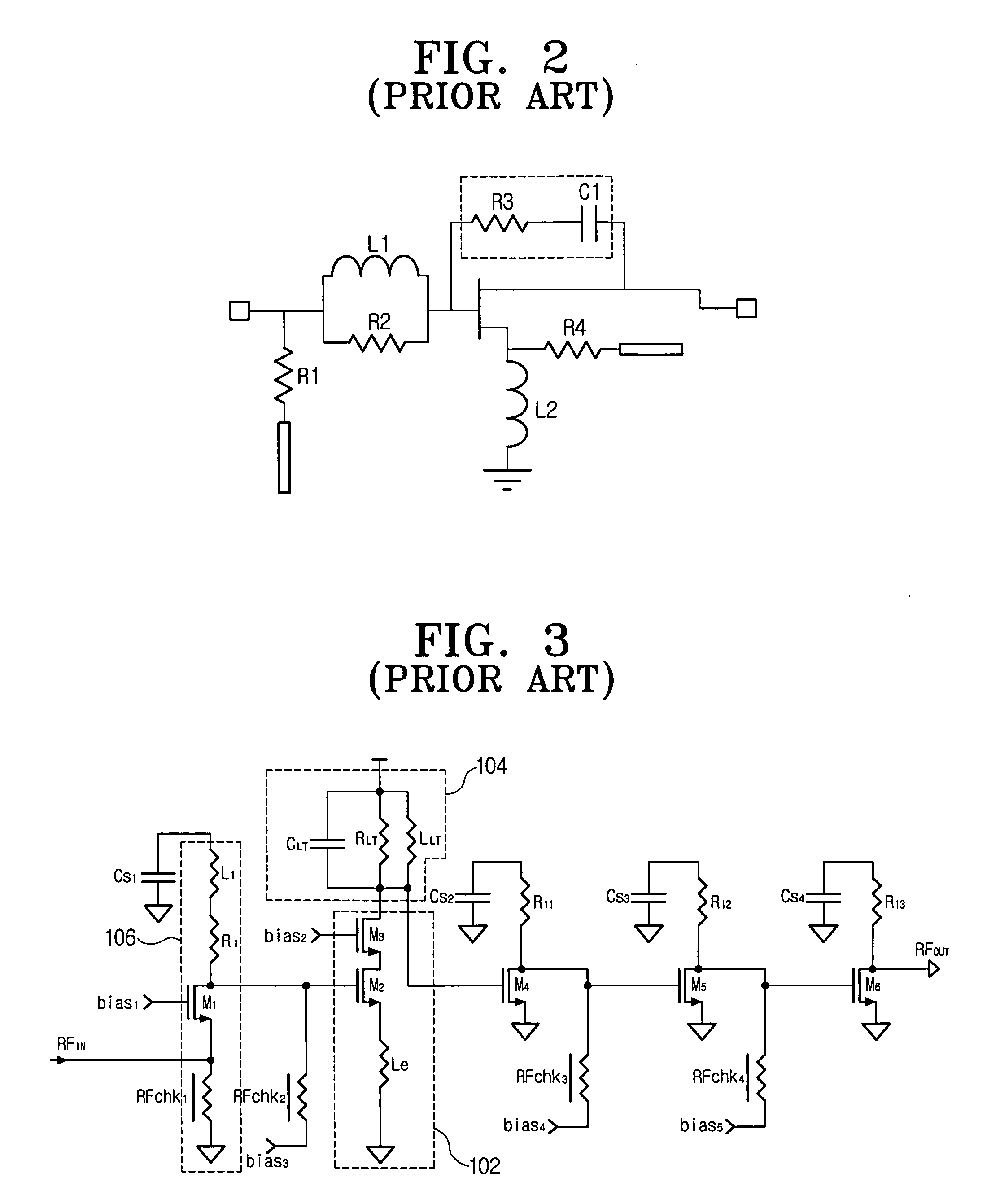
[0031] A general narrow band low noise amplifier (LNA), as shown in FIG. 4, employs inductors at a source and a gate of an amplifying element and thus generates an impedance input to the LNA up to 50 Ω.

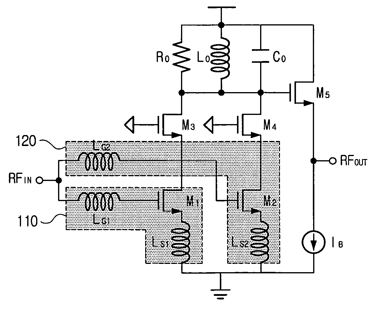
[0032] A LNA for ultra wide band (UWB) according to an embodiment of the present invention is designed by coupling narrow band LNAs in parallel.

[0033]FIG. 5 is a schematic circuit diagram of the LNA for the UWB acc...


PUM


Abstract

A low noise amplifier (LNA) for ultra wide band recives and amplifies identical RF signals in different frequency bands, and includes more than one pair of narrow band LNAs coupled in parallel, and a load circuit which increases load impedance of the entire circuit of the narrow band LNAs. The LNA can not only amplify the RF signal in the UWB but also obtain the low noise and the high gain that are features of the conventional narrow band LNA.

Description

CROSS-REFERENCE TO RELATED APPLICATIONS [0001] This application claims the benefit under 35 U.S.C. § 119(a) from Korean Patent Application No. 2005-9135 filed on Feb. 1, 2005 in the Korean Intellectual Property Office, the entire disclosure of which is incorporated herein by reference. BACKGROUND OF THE INVENTION [0002] 1. Field of The Invention [0003] Apparatuses consistent with the present invention relate to a low noise amplifier for ultra wide band. More particularly, the present invention relates to a low noise amplifier (LNA) for ultra wide band (UWB), which amplifies signals in the ultra wide band by coupling narrow band LNAs and thus obtains high gain and low noise figure (NF) which are characteristics of the narrow band LNA. [0004] 2. Description of The Related Art [0005] With the wide use of Internet and the rapid increase of multimedia data, there is a great demand for very high speed communication networks. Among those networks, a local area network (LAN) has been introd...

Claims


Application Information

Patent Timeline
IPC IPC(8): H03F1/22
CPCH03F1/223H03F1/26H03F1/42H03F1/483H03F3/211H03F3/345H03F2200/294H03F2200/36H03F2200/372H03F2200/39F16K17/194F16K27/02F16K31/0655
Inventor CHA, CHOONG-YULKIM, HOON-TAELEE, SANG-GUG
Owner SAMSUNG ELECTRONICS CO LTD
Why Eureka
Try Eureka