Array self repair using built-in self test techniques

a self-repair and array technology, applied in the field of array self-repair, can solve the problems of excessive chip real estate consumption, low device yield, and excessive test time and complex test software support algorithms

Inactive Publication Date: 2006-08-03
IBM CORP
View PDF17 Cites 8 Cited by
  • Summary
  • Abstract
  • Description
  • Claims
  • Application Information

AI Technical Summary

Problems solved by technology

These highly integrated circuit functions in conjunction with state-of-the-art semiconductor technology advances usually result in relatively low device yields unless redundancy compensation is an integral part of the overall design.
The problem addressed herein is encountered in the testing and determination of redundancy configurations for large numbers of small array macros in this ABIST and signature analysis design

Method used


Image

  • Array self repair using built-in self test techniques
  • Array self repair using built-in self test techniques
  • Array self repair using built-in self test techniques

Examples


Embodiment Construction

[0015] Reference will now be made to embodiments of the invention shown in the accompanying drawings. Where possible, the same reference numerals are used throughout the drawings to refer to the same or like parts.

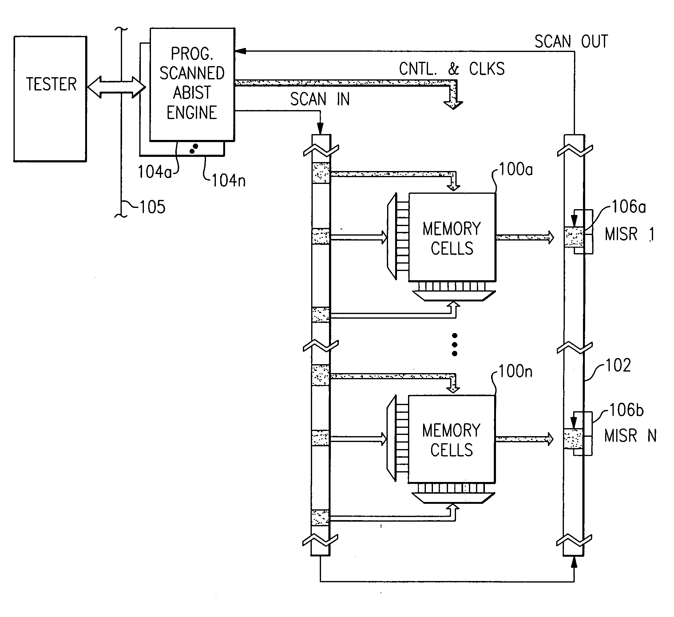
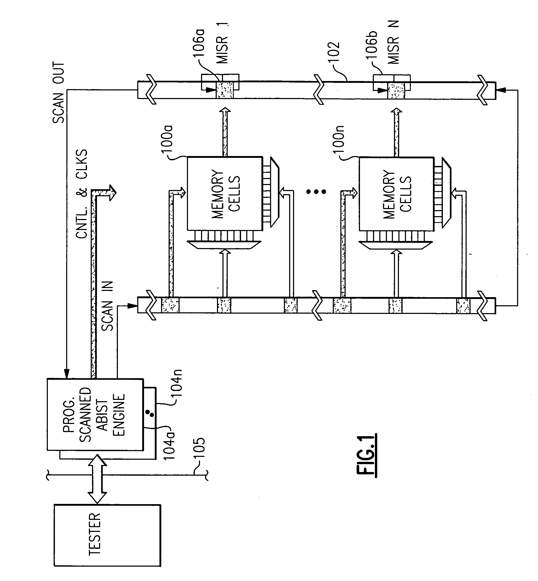
[0016] A typical Scanned ABIST configuration is depicted in FIG. 1. In this example, a number of arrays 100a to 100n are embedded within an integrated circuit design and accessed via a scan chain 102. On-chip ABIST engines 104a to 104n contain hard wired array test data (address, data, controls and clock signals) for all arrays 100. An off-chip tester 103 sets up the ABIST engine for testing, selects the test to be performed by the ABIST engines 104 and receives test results from the engines. The output responses for the arrays 100 are compressed into individual MISRs 106a to 106n which are also accessible via the scan chain 102. The ABIST engine 104a generates test patterns for testing the arrays 100 and seeds for the MISRs that result in the MISRs 106 of all good arrays...


PUM


Abstract

A soft-fuse test algorithm is distributed on-chip from an ABIST engine through an LSSD shift register chain to dynamically evaluate a plurality of arrays with redundancy compensation for bad elements and repair those that are fixable. Each arrays outputs are monitored by a different multiple input signature register (MISR) with an initial data pattern seed that provides a final desired state of the MISR with either all “0”s or all “1”s, allowing for a simple “single-bit” MISR error evaluation of the monitored array. Using the above single-bit MISR error evaluation technique an ABIST test sequence is executed concurrently on all arrays through the shift register chain. If any arrays are in error, redundancy compensation is employed and the ABIST test is repeated for all possible array redundant combinations until a functional configuration for each array is identified or all possible redundant combinations have been tried. Once functioning array configurations are verified, the associated soft-fuse states can be used to blow fuses and/or extracted for further system setup, permanent fuse-blowing and yield analysis. Multiple shift register chains driven by separate ABIST engines may be required to test all arrays on a chip.

Description

RELATED APPLICATIONS [0001] U.S. patent application, Ser. No. 10 / 721,646, filed Nov. 25, 2003 and entitled “System and Method for Testing Electronic Devices on a Microchip” is hereby incorporated by reference.FIELD OF THE INVENTION [0002] The present invention relates to testing of arrays embedded in complex logic circuits embodied in large scale integration (LSI) and very large scale integration (VLSI) circuit devices and more particularly, to the diagnosing and repair of such arrays. BACKGROUND OF THE INVENTION [0003] The density of very large scale integration (VLSI) devices, incorporating complex functions operating at extreme circuit performances, has driven designers to integrate many diverse memory array macros within these devices. These memory macros range from large cache arrays occupying relatively large portions of the chip's real estate, to a multitude of small arrays used as register stacks, trace arrays, content addressable memories (CAMs), and many other special purp...

Claims


Application Information

Patent Timeline
IPC IPC(8): G01R31/28
CPCG01R31/318566G01R31/318572
Inventor HUOTT, WILLIAM V.MOTIKA, FRANCOPATEL, PRADIPRODKO, DANIEL
Owner IBM CORP
Why Eureka
Try Eureka