Process condition sensing wafer and data analysis system

a technology of data analysis and processing condition, applied in the direction of semiconductor/solid-state device testing/measurement, simultaneous indication of multiple variables, instruments, etc., can solve the problems of failure completely, failure substandard performance of subsequent integrated circuit or device, etc., to achieve repeatable, drift-free operation, and wide operating range.

Inactive Publication Date: 2006-08-10
KLA TENCOR TECH CORP
View PDF58 Cites 57 Cited by
  • Summary
  • Abstract
  • Description
  • Claims
  • Application Information

AI Technical Summary

Benefits of technology

[0009] Distancing sensitive electronic circuitry from the processing conditions results in

Problems solved by technology

Any deviation from optimal processing conditions may cause the ensuing integrated

Method used


Image

  • Process condition sensing wafer and data analysis system
  • Process condition sensing wafer and data analysis system
  • Process condition sensing wafer and data analysis system

Examples


Embodiment Construction

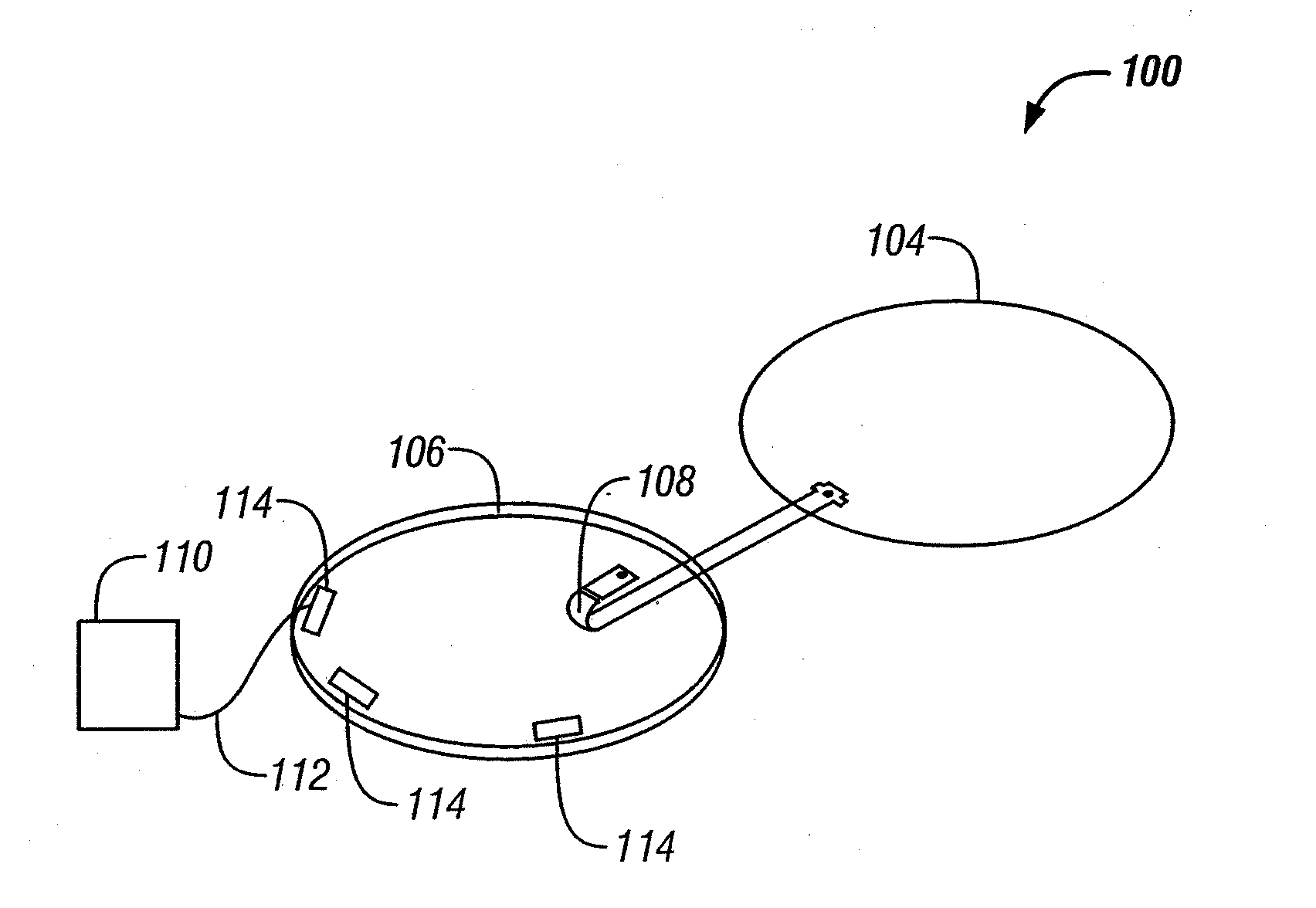
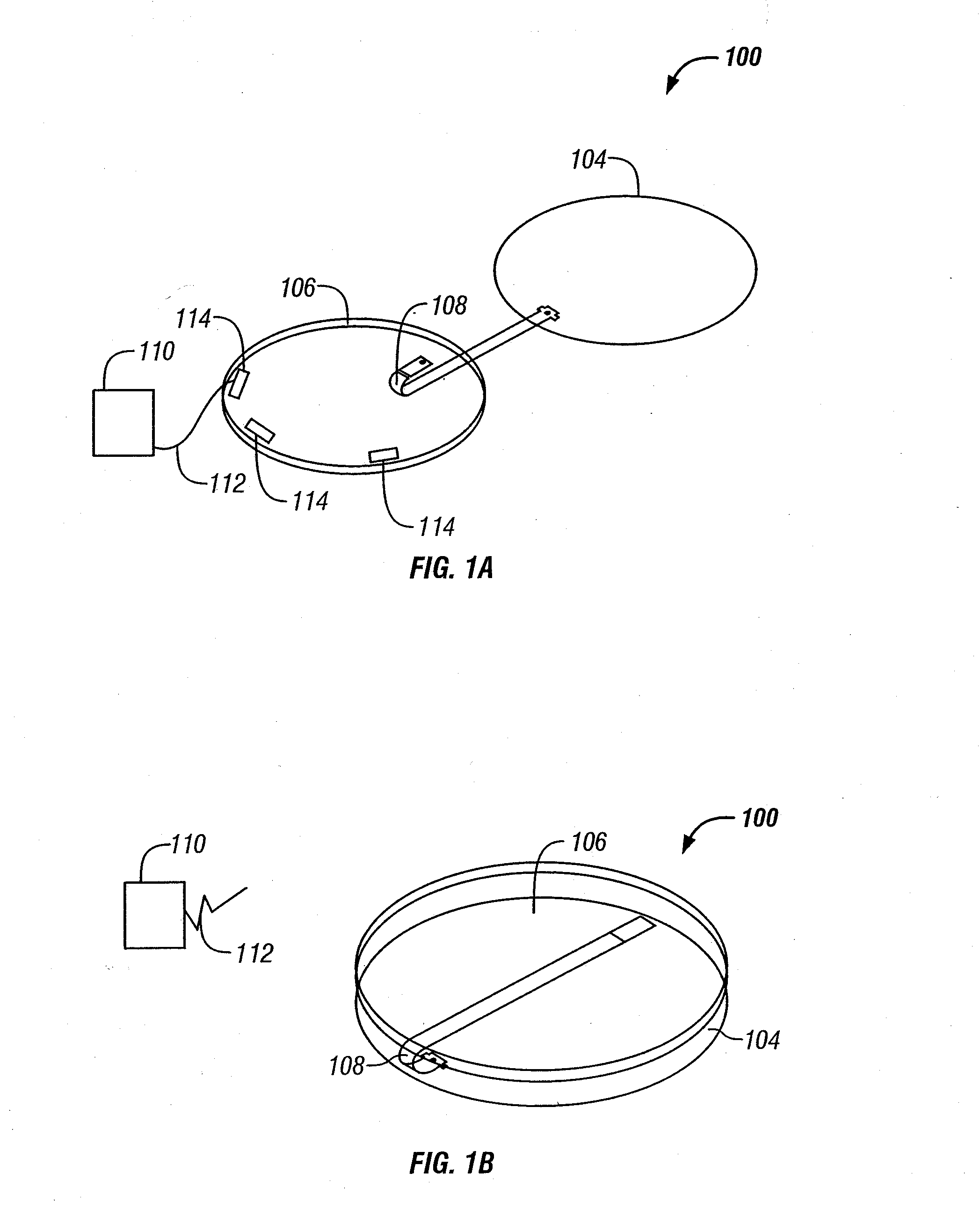
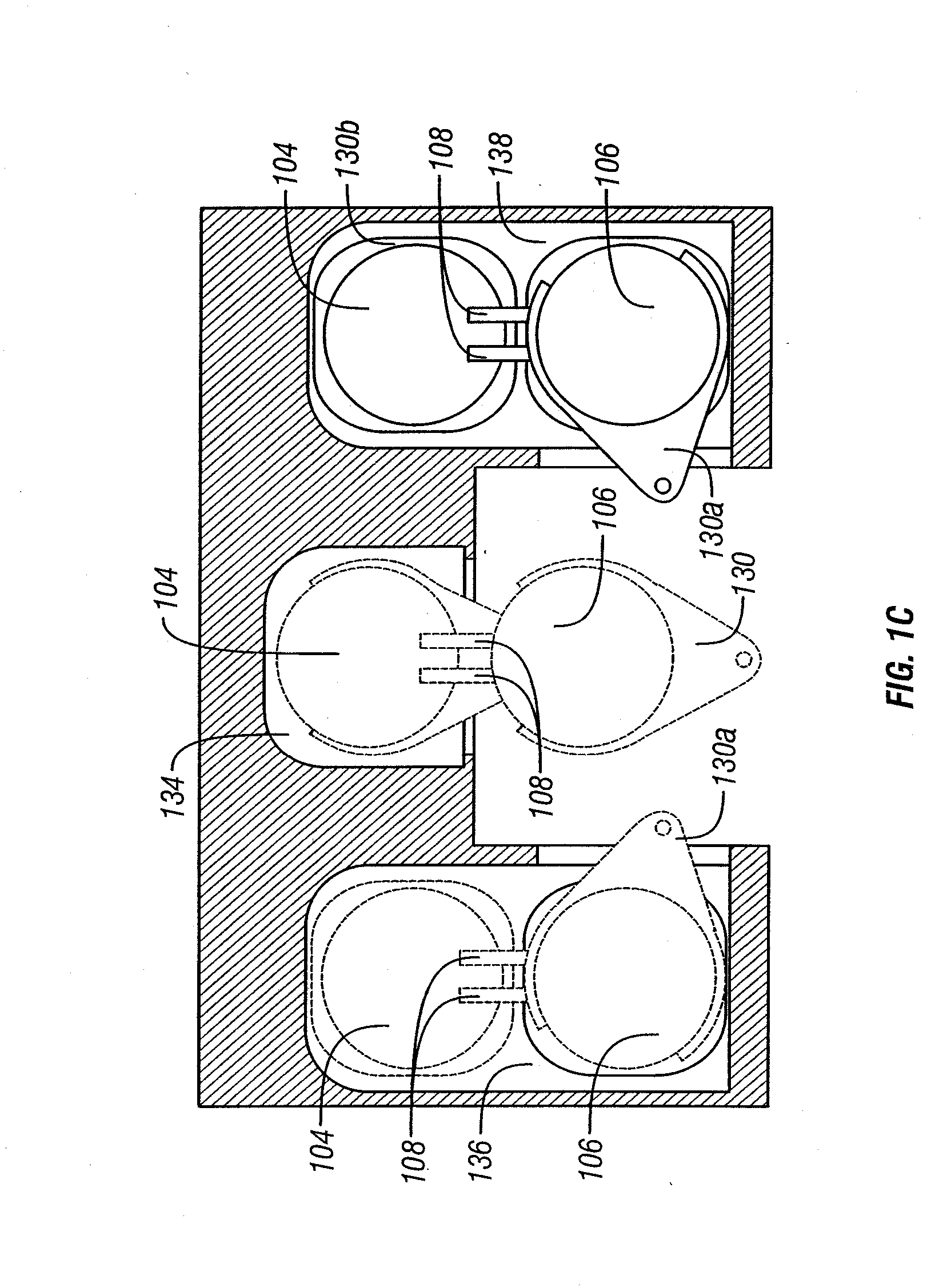
[0037] The measurement system of the present invention measures processing conditions in various locations of a wafer or substrate and transmits them in real time to a data processing device or records them in memory for later transmission or downloading of process conditions.

[0038] As defined herein, “processing conditions” refer to various processing parameters used in manufacturing an integrated circuit. Processing conditions include any parameter used to control semiconductor manufacture or any condition a manufacturer would desire to monitor such as but not limited to temperature, processing chamber pressure, gas flow rate within the chamber, gaseous chemical composition within the chamber, ion current density, ion current energy, light energy density, and vibration and acceleration of the wafer.

[0039] The invention will now be described with reference to the figures.

[0040]FIG. 1A illustrates processing condition measuring device (“PCMD”) 100, a first embodiment of the inven...


PUM

PropertyMeasurementUnit
Angleaaaaaaaaaa
Angleaaaaaaaaaa
Angleaaaaaaaaaa

Abstract

A measuring device incorporating a substrate with sensors that measure the processing conditions that a wafer may undergo during manufacturing. The substrate can be inserted into a processing chamber by a robot head and the measuring device can transmit the conditions in real time or store the conditions for subsequent analysis. Sensitive electronic components of the device can be distanced or isolated from the most deleterious processing conditions in order increase the accuracy, operating range, and reliability of the device. Isolation may be provided by vacuum or suitable material and phase change material may be located adjacent to electronics to maintain a low temperature.

Description

CROSS-REFERENCE TO RELATED APPLICATIONS [0001] This application is a continuation-in-part of application Ser. No. 10 / 685,550, filed Oct. 14, 2003; which application is a divisional of application Ser. No. 10 / 056,906, filed Jan. 24, 2002, now U.S. Pat. No. 6,889,568. These applications are incorporated by reference as if fully set forth herein.BACKGROUND OF THE INVENTION [0002] 1. Field of the Invention [0003] The present invention relates to a semiconductor wafer processing, LCD display glass substrate processing, magnetic memory disc processing and other devices fabricated from thin film processes and more specifically to a substrate which can sense and transmit processing conditions. [0004] 2. Discussion of the Related Art [0005] The fabrication of an integrated circuit, display or disc memory generally employs numerous processing steps. Each process step must be carefully monitored in order to provide an operational device. Throughout the imaging process, deposition and growth pr...

Claims


Application Information

Patent Timeline
IPC IPC(8): G01D7/02G01M99/00
CPCG01D9/005H01L21/67253H01L22/34Y10T29/4913H01L2224/48091H01L2924/00014
Inventor RENKEN, WAYNE G.SUN, MEI H.
Owner KLA TENCOR TECH CORP
Why Eureka
Try Eureka