Multi-layer polymeric electronic device and method of manufacturing same

a polymeric electronic device and polymer technology, applied in the direction of electrical apparatus construction details, fixed capacitor details, positive temperature coefficient thermistors, etc., can solve the problem of reducing manufacturing costs and achieve the effect of high space-saving

Inactive Publication Date: 2006-08-10
BOURNS INC
View PDF7 Cites 36 Cited by
  • Summary
  • Abstract
  • Description
  • Claims
  • Application Information

AI Technical Summary

Benefits of technology

[0010] As will be appreciated from the detailed description below, the present invention provides a cost-efficient method of manufacturing multi-layer laminar electronic components that are also highly space-efficient. Moreover, the method of the invention offers a great deal of flexibility in manufacturing devices of a wide variety of electrical properties and characteristics in a single, space-saving package that is, preferably, vertically and / or laterally symmetrical, thereby resulting in advantages in installing the devices on circuit boards using conventional pick-and-place machinery. These and other advantages will be more fully understood from the following detailed description.

Problems solved by technology

Heretofore, however, the need to create inter-layer conductive paths has presented challenges in reducing manufacturing costs, and thus more cost-efficient manufacturing methods are continually being sought.

Method used


Image

  • Multi-layer polymeric electronic device and method of manufacturing same
  • Multi-layer polymeric electronic device and method of manufacturing same
  • Multi-layer polymeric electronic device and method of manufacturing same

Examples


Embodiment Construction

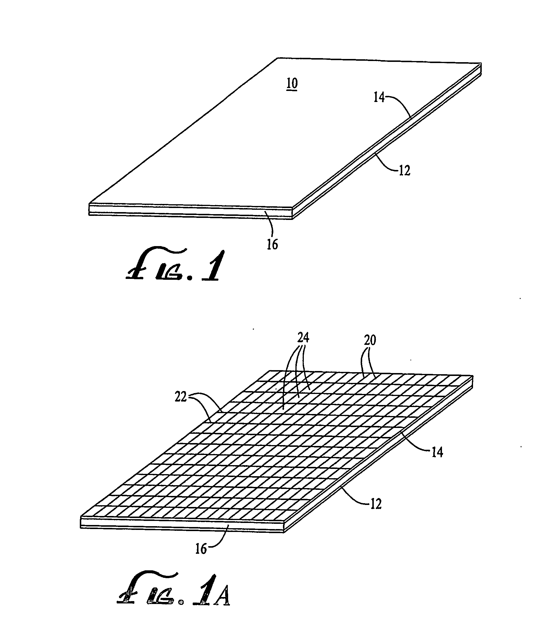
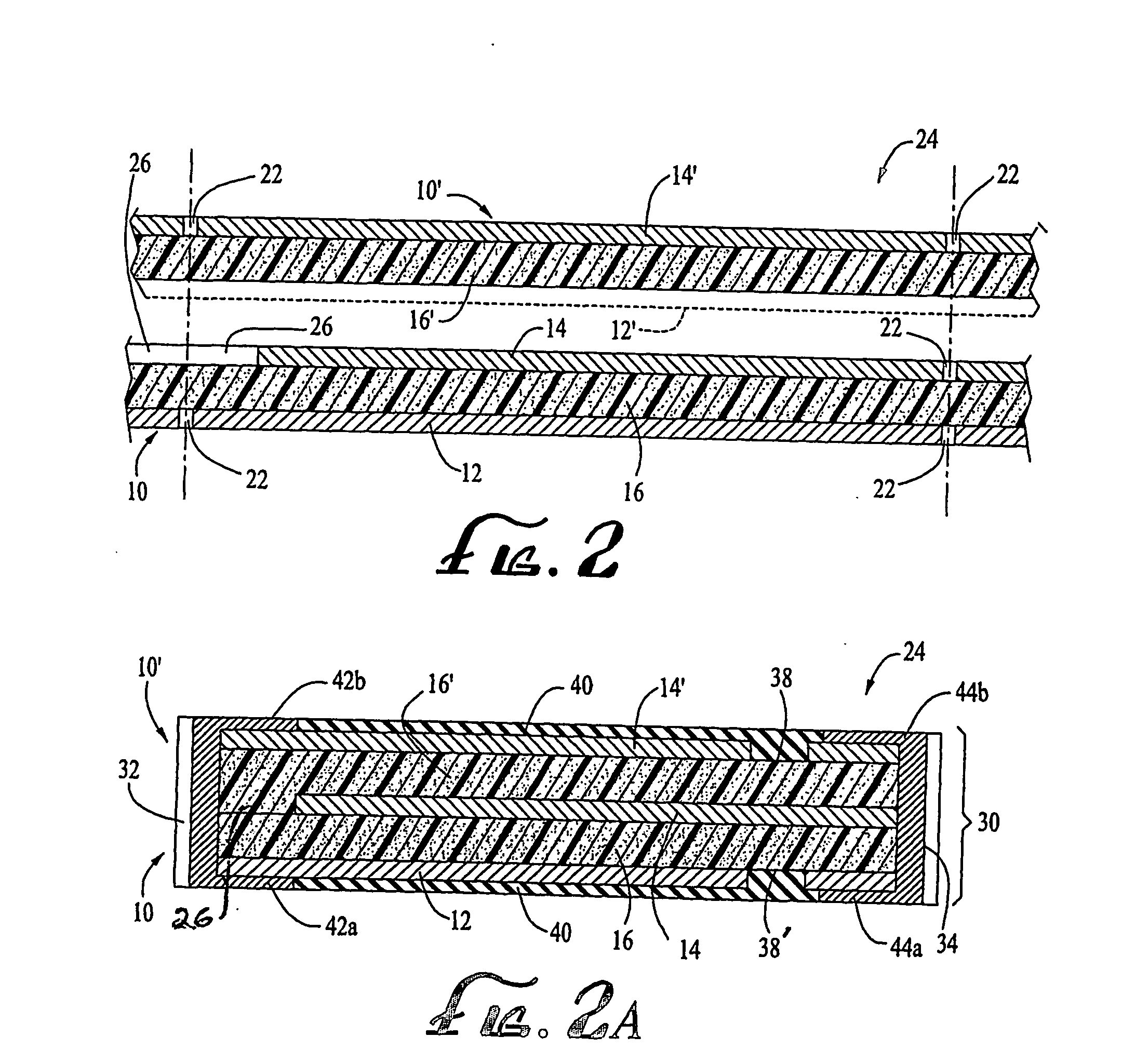
[0030] The various embodiments of the present invention are made with one or more laminated sheet structures, of the type shown in FIG. 1. As shown, a laminated sheet structure 10 comprises a layer of polymeric active material 16 laminated between a lower laminar metal layer 12 and an upper laminar metal layer 14. The polymeric layer 16 may be a conductive polymer, such as a polymeric positive temperature coefficient (PTC) resistive material, or it may be a polymeric dielectric material, or a ferromagnetic polymer. Various types of suitable polymer materials are well-known in the art. The metal layers 12, 14 are preferably made of conductive metal foil, and more preferably a nickel-plated copper foil that is nodularized (by conventional techniques) on the surface that is placed against the polymeric layer. The lamination may be performed by any suitable lamination process known in the art, an example of which is described in International Patent Publication No. WO 97 / 06660, the disc...


PUM

PropertyMeasurementUnit
non-metallicaaaaaaaaaa
non-metallic aaaaaaaaaa
distanceaaaaaaaaaa

Abstract

An electronic device is formed of multiple, alternating layers of conductive polymer and metal foil electrodes, in which electrical connections between selected electrodes are provided by cross-conductors formed by plated through-hole vias. More specifically, the device includes a first cross-conductor that electrically connects a first set of electrodes, and a second cross-conductor electrically connects a second set of electrodes. Correspondingly, the first cross-conductor is electrically and physically isolated from the second set of electrodes, while the second cross-conductor is electrically and physically isolated from the first set of electrodes. The electrodes are etched to form an isolation gap that isolates that electrode from either the first or second cross-conductor. The first and second cross-conductors, in turn, are formed by plating the through-hole vias, so as to establish electrically-conductive contact with those electrodes not separated from the via by an isolation gap. Thus, a device may be formed with N non-metallic (e.g. polymeric) layers and N+1 electrodes, where N is an integer greater than 1, wherein a first cross-conductor electrically contacts a first set of electrodes, and a second cross-conductor electrically contacts a second set of electrodes, whereby the non-metallic layers are connected in parallel.

Description

CROSS-REFERENCE TO RELATED APPLICATION [0001] This application claims the benefit, under 35 U.S.C. Section 119(e), of co-pending U.S. Provisional Application No. 60 / 454,754, filed Mar. 14, 2003, the disclosure of which is incorporated herein by reference.FEDERALLY SPONSORED RESEARCH OR DEVELOPMENT [0002] Not Applicable BACKGROUND OF THE INVENTION [0003] The present invention relates to a multi-layer polymeric electronic device or component and a method of manufacturing it. Specifically, the present invention relates (a) to a method of manufacturing multi-layer polymeric electronic devices using a process that employs plated through-hole vias to create conductive paths between selected laminar electrodes; and (b) to a multi-layer polymeric electronic device made in accordance with the method of the invention. More specifically, the invention relates to a laminar electronic device comprising two or more polymeric active elements laminated between laminar metal (e.g., foil) layers that...

Claims


Application Information

Patent Timeline
Patent Type & Authority Applications(United States)
IPC IPC(8): H05K7/06H05K3/36H05K1/03H01C1/148H01C7/02H01C7/18H01G4/232
CPCH01C1/1406H01C1/148H01C1/16H01C7/021H01C7/027H01C7/18Y10T29/49165H05K3/0052H05K3/403H05K3/429H05K2201/09181Y10T29/49126H01G4/232
Inventor BOURNS, GORDONSTRAKER, GARYBURKE, RAYNGUYEN, THANH
Owner BOURNS INC
Why Eureka
Try Eureka