Method for fabricating interconnection in an insulating layer on a wafer and structure thereof

a technology of interconnection and insulating layer, which is applied in the manufacturing of semiconductor/solid-state devices, basic electric elements, electric devices, etc., can solve the problems of significant increase in the overall yield of the wafer, troublesome rework, and high cost of the fib device, so as to reduce the repairing cost

Inactive Publication Date: 2006-08-10
UNITED MICROELECTRONICS CORP
View PDF3 Cites 0 Cited by
  • Summary
  • Abstract
  • Description
  • Claims
  • Application Information

AI Technical Summary

Benefits of technology

[0006] Accordingly, at least one objective of the present invention is to provide a method for fabricating an inte...

Problems solved by technology

This kind of operational mode not only saves the trouble of producing rework photomask and some other costs, but also significantly increases overall yield of the wafer.
However, there are a still a few drawbacks in using the FIB technique to repair wafer circuits.
Because a FIB device is an expensive piece o...

Method used


Image

  • Method for fabricating interconnection in an insulating layer on a wafer and structure thereof
  • Method for fabricating interconnection in an insulating layer on a wafer and structure thereof
  • Method for fabricating interconnection in an insulating layer on a wafer and structure thereof

Examples


Embodiment Construction

[0023] Reference will now be made in detail to the present preferred embodiments of the invention, examples of which are illustrated in the accompanying drawings. Wherever possible, the same reference numbers are used in the drawings and the description to refer to the same or like parts.

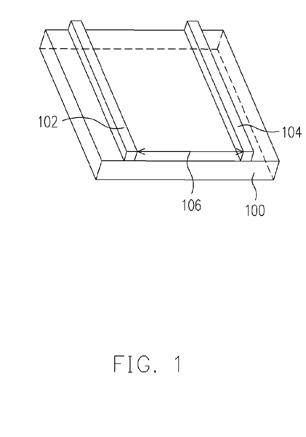
[0024] In the past, the circuits on a wafer are repaired using the conventional focused ion beam (FIB) technique. However, the FIB technique of wafer circuit repair requires a relatively long repairing period and a high repairing cost. In particular, the repairing time and cost using the conventional FIB technique will be exceedingly high as shown in FIG. 1 if the distance 106 separating the conductive lines 102 and 104 on the wafer 100 is long over hundreds of micrometers.

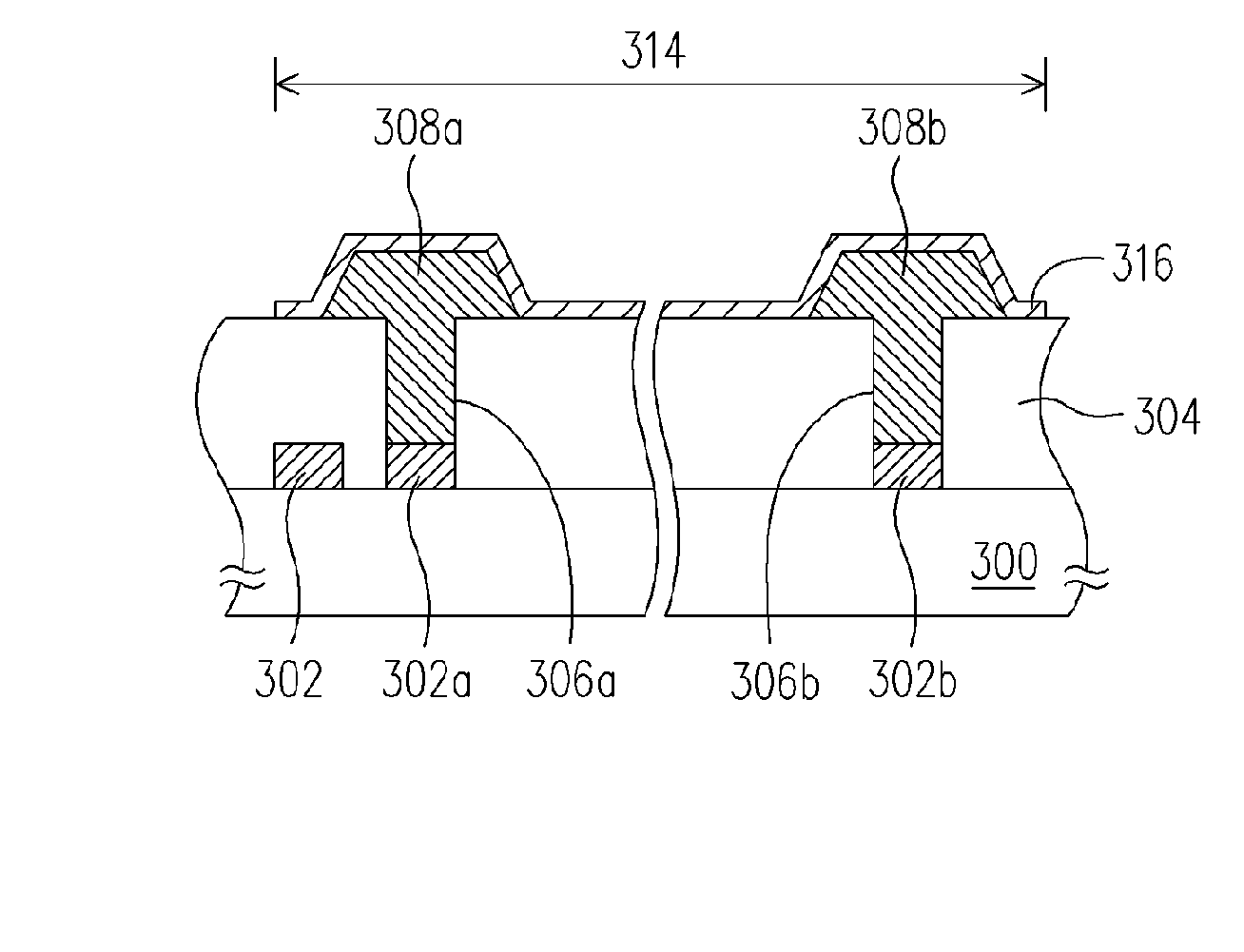
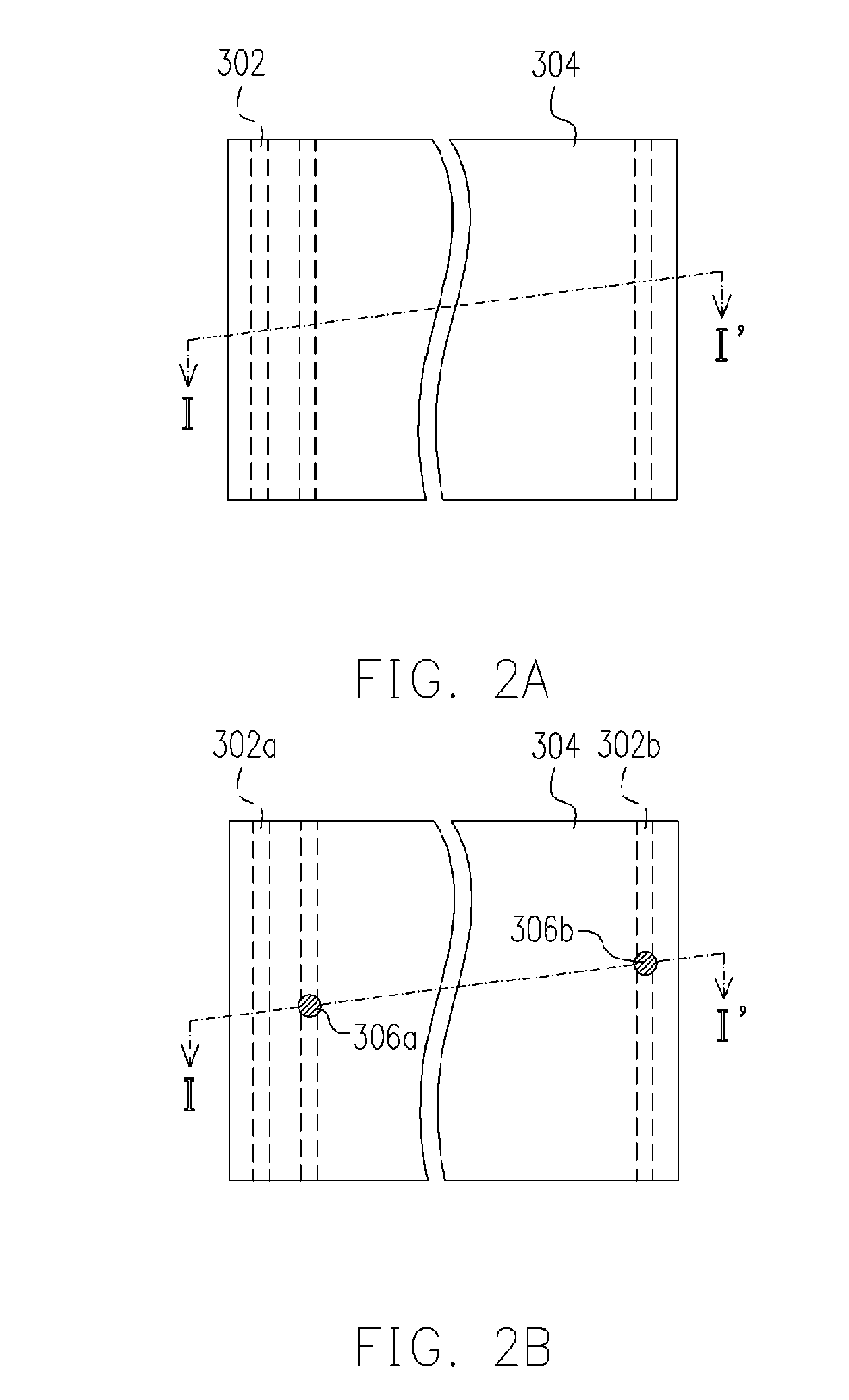
[0025]FIGS. 2A through 2F are top views showing the steps for fabricating an interconnection in an insulating layer on a wafer according to one preferred embodiment of the present invention. FIGS. 3A through 3F are schematic cro...


PUM


Abstract

A method for fabricating an interconnection in an insulating layer on a wafer is described. A wafer having a plurality of conductive lines thereon is provided. An insulating layer is formed over the conductive lines. Two via holes are formed in the insulating layer to expose two of the conductive lines waiting to be repaired. A first conductive layer is filled into the via holes to form two pattern marks. A mask is formed over the wafer to cover the insulating layer and the two pattern marks. The mask located above and between the two pattern marks is removed to form a trench exposing the two pattern marks and a portion of the insulating layer. A second conductive layer is formed over the mask to cover the two exposed pattern marks and the exposed insulating layer. The mask and the second conductive layer above the mask are removed simultaneously.

Description

BACKGROUND OF THE INVENTION [0001] 1. Field of the Invention [0002] The present invention relates to a semiconductor process. More particularly, the present invention relates to a method of fabricating an interconnection in an insulating layer on a wafer and a structure thereof. [0003] 2. Description of the Related Art [0004] Integrated circuit fabrication is a high-tech industry that involves four major subsystems including integrated circuit design, wafer manufacturing, wafer testing and wafer packaging. After all the steps necessary for fabricating a complete integrated circuit have been completed, a series of tests is carried out to ensure the quality of the final products and / or to modify the circuit fabrication process according to the test results. Furthermore, at the end of a wafer fabrication cycle, the wafer frequency undergoes many types of wafer tests. If defects or out-of-spec elements are found in the circuit on the wafer, a repair operation is often carried out to for...

Claims


Application Information

Patent Timeline
IPC IPC(8): H01L21/30
CPCH01L21/76892
Inventor LIN, STEVEN GSCHIU, SU-PING
Owner UNITED MICROELECTRONICS CORP
Why Eureka
Try Eureka