Ultra-small Profile, Low Cost Chip Scale Accelerometers of Two and Three Axes Based on Wafer Level Packaging
a technology of chip scale and accelerometer, which is applied in the direction of speed/acceleration/shock measurement, measurement devices, instruments, etc., can solve the problem of adding expense to their often cost-sensitive products
- Summary
- Abstract
- Description
- Claims
- Application Information
AI Technical Summary
Problems solved by technology
Method used
Image
Examples
Embodiment Construction
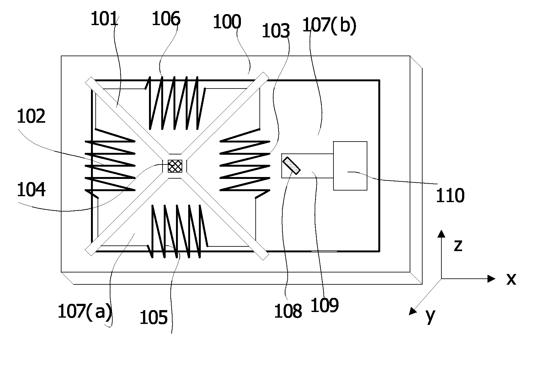
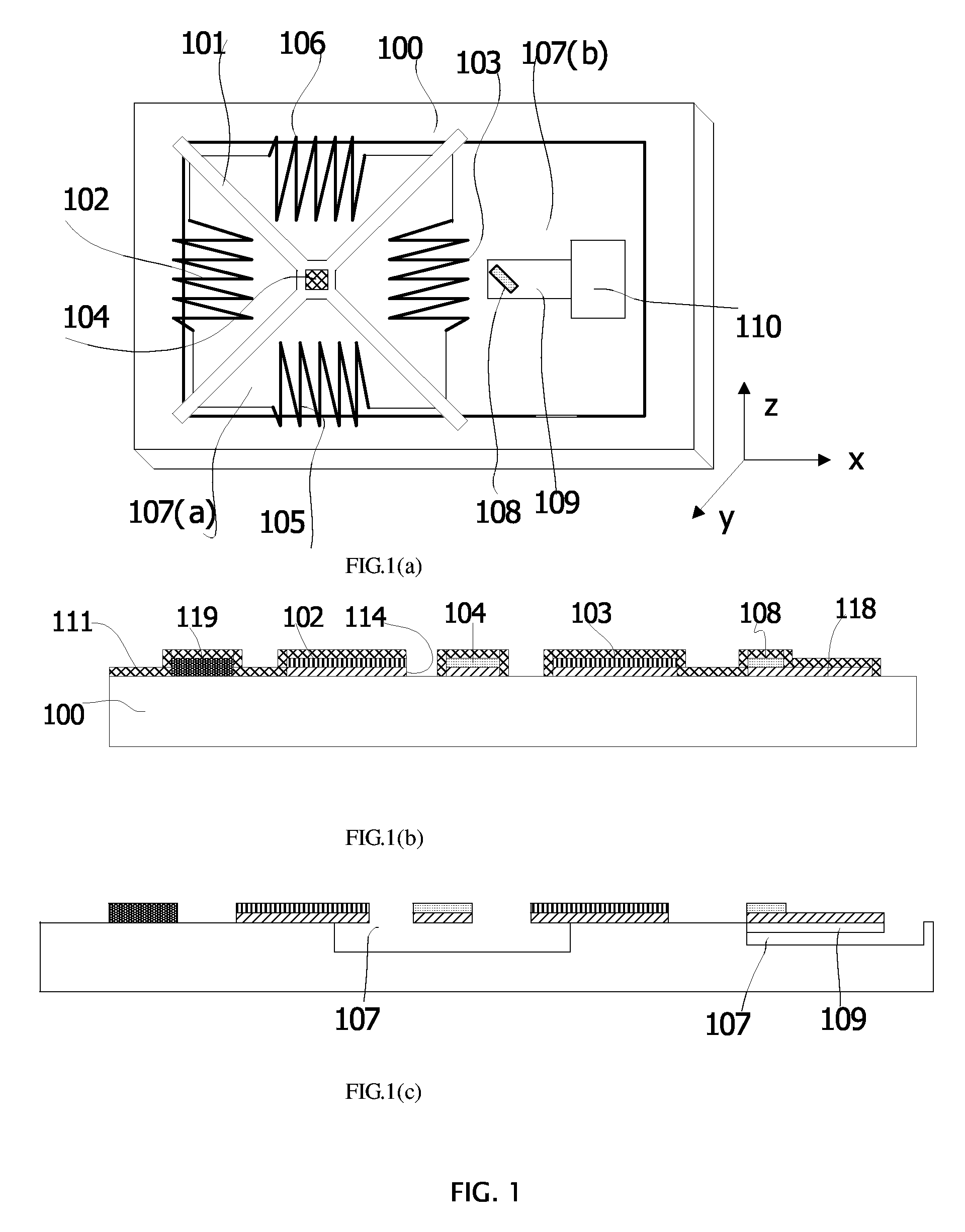
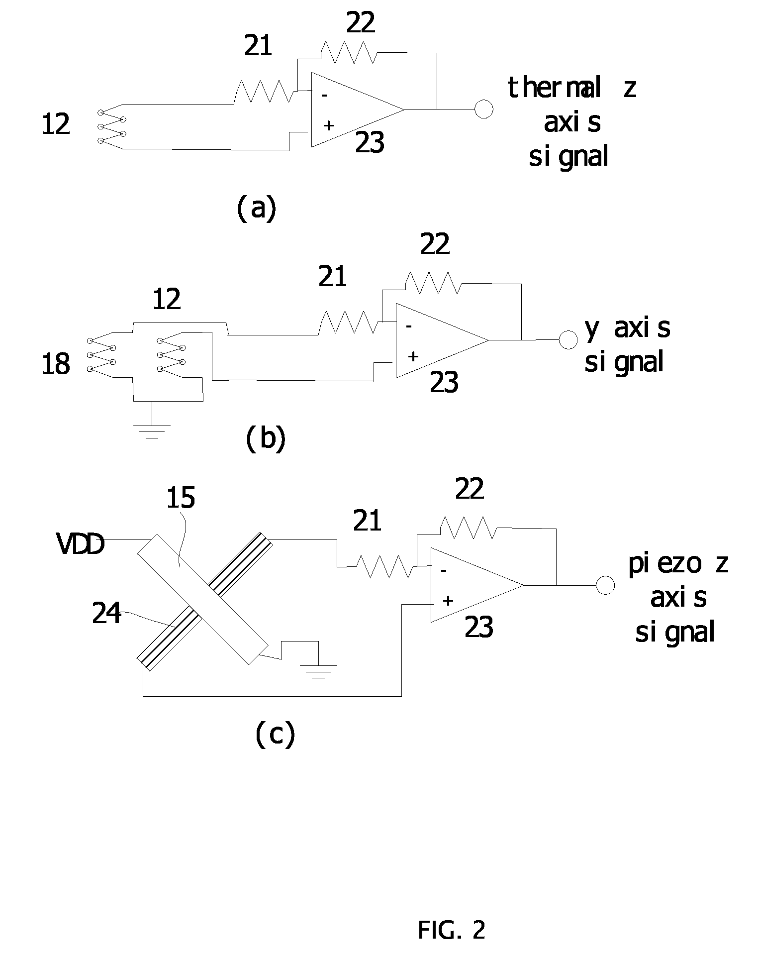
[0010] Referring to FIG. 1(a), the accelerometer is formed on a silicon substrate 100 in which a cavity 107 is formed underneath a heater 104 and thermopiles 102,103,105,106. The thermopiles arranged in two orthogonal directions are thermopiles with each thermopile in one pair at a distance of about x / D=0.2 to achieve larger sensitivity. The heater 104 is implemented using four short resisters made of polysilicon arranged in a small square. The heater 104 and two pairs of thermopiles are all suspended above the cavity 107 with four metal bridges 101 formed by aluminum. Electrical current passing through the heater104 via the four-bridge connection to external power source, and then the temperature of the gas around the heater is increased and temperature gradient is established. “T-shape” distribution proof mass 110 is also above another cavity, with beam 109 and piezoresistor 108 comprising a z-axis accelerometer. When z-axis acceleration is applied on the sensor, the beam will ben...
PUM
 Abstract
Description
Claims
Application Information


