Semiconductor memory device for low voltage

Inactive Publication Date: 2006-08-17
SK HYNIX INC
View PDF23 Cites 390 Cited by
  • Summary
  • Abstract
  • Description
  • Claims
  • Application Information

AI Technical Summary

Benefits of technology

[0058] It is, therefore, an object of the present invention to provide a semiconductor memory

Problems solved by technology

However, on the nano-technology based on under 100 nm, it is very difficult to develop the nano-technology.
That is, there is a limitation for integrating the semiconductor memory device more and more.
Also, a requested voltage level of the power supply voltage becomes lower, e.g., from about 2.0 V to about 1.5 V or so far as about 1.0 V. Thus, the request about the power supply voltage cannot be achieved by only developing the nano-technology.
If a voltage level of the power supply voltage inputted to the semiconductor memory device is lower than a predetermined voltage level, an operating margin of each transistor included in the semiconductor memory device is not sufficient; and, as a result, a requested operation speed is not satisfied and an operatio

Method used


Image

  • Semiconductor memory device for low voltage
  • Semiconductor memory device for low voltage
  • Semiconductor memory device for low voltage

Examples


Embodiment Construction

[0081] Hereinafter, a semiconductor memory device in accordance with the present invention will be described in detail referring to the accompanying drawings.

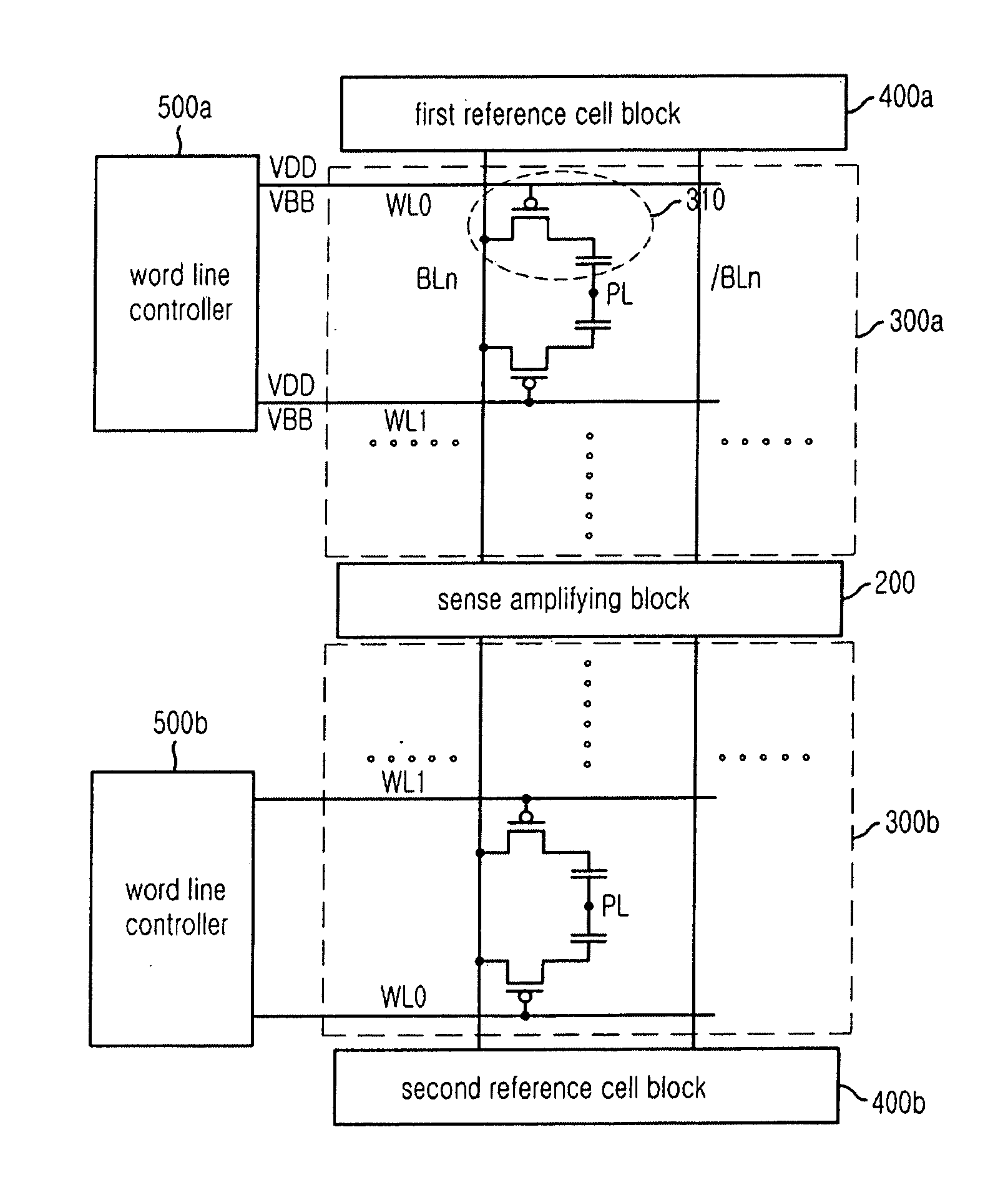
[0082]FIG. 7 is a block diagram showing a semiconductor memory device in accordance with an embodiment of the present invention.

[0083] As shown, the semiconductor memory device includes a plurality of cell arrays, e.g., 300a and 300b, a plurality of sense amplifying blocks, e.g., 200. The semiconductor memory device further includes word line controllers, e.g., 500a and 500b, and reference cell blocks, e.g., 400a and 400b, corresponding to the cell arrays.

[0084] In detail, each cell array, e.g., 300a, includes a plurality of unit cells, e.g., 310, each provided with a PMOS transistor and a capacitor. The PMOS transistor included in each unit cell connected to a corresponding word line WL0 and WL1, driven based on a low voltage VBB and a power supply voltage VDD.

[0085] The word line controller 500a and 500b, determines a vol...


PUM


Abstract

A semiconductor memory device includes a first cell array including a plurality of unit cells and a bit line sense amplifying unit for sensing and amplifying data signals stored in the unit cells. Each unit cell is provided with a PMOS transistor and a capacitor. Therefore, the semiconductor memory device efficiently operates with low voltage without any degradation of operation speed.

Description

FIELD OF THE INVENTION [0001] The present invention relates to a semiconductor memory device; and, more particularly, to a semiconductor memory device for efficiently operating under a low power supply voltage condition. DESCRIPTION OF RELATED ARTS [0002]FIG. 1 is a block diagram describing a conventional semiconductor memory device. [0003] As shown, the conventional semiconductor memory device includes a row address decoder 20, a column address decoder 30, a cell area 100 and a data input / output block 40. [0004] The cell area 100 includes a plurality of cell arrays, e.g., 110, 120, 130 and 140 and a plurality of sense amplifying blocks, e.g., 150 and 160. The row address decoder 20 receiving a row address decodes the row address in order to access a data stored in the cell area 100. The column address decoder 30 receiving a column address decodes the column address in order to access the data stored in the cell area 100. The data input / output block 40 is for outputting a data store...

Claims


Application Information

Patent Timeline
IPC IPC(8): G11C11/24
CPCG11C7/065G11C7/14G11C7/18G11C11/4091G11C11/4097G11C11/4099G11C2207/005G11C7/06G11C2207/2227
Inventor KANG, HEE-BOKAHN, JIN-HONGLEE, SANG-DON
Owner SK HYNIX INC
Why Eureka
Try Eureka