Non-volatile memory device and method for operation page buffer thereof

Inactive Publication Date: 2006-08-17
SK HYNIX INC
View PDF8 Cites 28 Cited by
  • Summary
  • Abstract
  • Description
  • Claims
  • Application Information

AI Technical Summary

Benefits of technology

[0011] According to embodiments of the present invention, there is provided a non-volatile memory device capable of eliminating errors and reducing copy-back program operation time b

Problems solved by technology

In the above-mentioned copy-back program operation, there is a high probability that errors occur in transmitting data between the first la

Method used


Image

  • Non-volatile memory device and method for operation page buffer thereof
  • Non-volatile memory device and method for operation page buffer thereof
  • Non-volatile memory device and method for operation page buffer thereof

Examples


Example

[0022] The present invention will be described below in more detail using specific embodiments and the accompanying drawings. The present invention may, however, be embodied in different forms and should not be construed as being limited to the embodiments set forth herein. Rather, these embodiments are provided for illustrative purposes to those skilled in the art. Like numerals refer to like elements.

[0023] Hereinafter, the invention will be described with reference to an exemplary embodiment of the present invention in conjunction with the accompanying drawings.

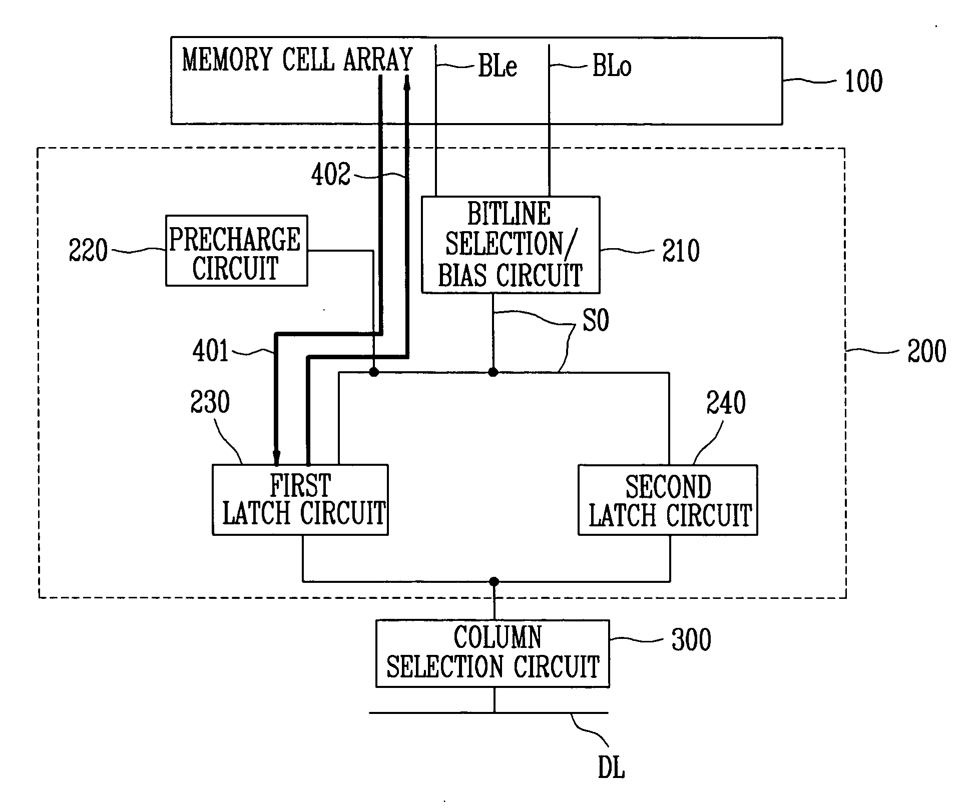
[0024]FIG. 3 is a block diagram illustrating a copy-back program operation of a NAND-type flash memory device according to a preferred embodiment of the present invention.

[0025] With reference to FIG. 3, a copy-back program operation is performed as follows. Data is read out from a defective cell by charging a sensing line S0 utilizing a precharging unit 220 to store the read out data in a first latch unit 230 (step S40...


PUM


Abstract

A non-volatile memory device includes a memory cell array including memory cells, each memory cell being defined at an intersection of a word line and a bit line. A page buffer is coupled to the memory cell array via a sensing line. The page buffer comprises a first latch unit including a first latch circuit and coupled to the sensing line, the first latch unit being configured to be activated during a copy-back program operation to read data stored in a first memory cell and reprogram the data to a second memory cell that is different from the first memory cell. The page buffer also includes a second latch unit including a second latch circuit and coupled to the sensing line, the second latch unit being configured not to be activated during the copy-back operation and be activated during program, read, and verification operations, the second latch unit configured to receive data to be programmed in the memory cells and store the data during the program operation, the second latch unit configured to read the data programmed in the memory cells and store the read data during the read and verification operations.

Description

BACKGROUND OF THE INVENTION [0001] The present invention relates to non-volatile memory devices and methods for operating them. More particularly it relates to a NAND-type flash memory device capable of shortening a copy-back program time by changing an operation of a page buffer, and a method for operating the page buffer. [0002] Recently, there has been increasing demand for semiconductor memory devices which do not require periodic refresh operations and are electrically programmable and erasable. A program operation writes data to the memory cells. [0003] To achieve high integration of semiconductor memory devices, NAND-type flash memory devices have a plurality of memory cells that share a common connection. In other words, neighboring cells share a drain and source with each other. Unlike NOR-type flash memory cells, NAND-type flash memory cells are capable of reading out information sequentially. [0004] NAND-type flash memory devices employ a page buffer in order to store lar...

Claims


Application Information

Patent Timeline
IPC IPC(8): G11C16/04
CPCG11C16/0483G11C16/10G11C16/105G11C16/3404G11C16/3431A44B19/00A45D29/20A45D44/04A45D2033/001A46B9/021
Inventor CHA, JAE WON
Owner SK HYNIX INC
Why Eureka
Try Eureka