Solid state imaging device, method of driving solid state imaging device, and image pickup apparatus

a solid-state imaging and imaging device technology, applied in the direction of radio frequency controlled devices, television systems, instruments, etc., can solve the problems of photocharge overflow, adversely affecting the pixels around the pixels, and the frame rate is not increased, so as to prevent the charge from continuing to accumulate

Inactive Publication Date: 2006-08-24
SONY CORP
View PDF8 Cites 19 Cited by
  • Summary
  • Abstract
  • Description
  • Claims
  • Application Information

AI Technical Summary

Benefits of technology

[0013] In the solid state imaging device described above, when a mode for selectively scanning only rows in a given clipping-out row range in the pixel array section and clipping and reading out pixel signals in the clipping-out row range is set, for the rows outside the given clipping-out row range, charges generated in the photoelectric conversion elements are discharged to the pixel power supply. Consequently, it is possible to prevent charges from continuing to be accumulated in the photoelectric conversion elements even if selective scanning is not applied to the rows outside the clipping-out row range.

Problems solved by technology

Finally, the photocharges overflow to adversely affect pixels around the pixels.
However, when the selective scanning is applied to the rows outside the clipping-out row range after selectively scanning only the respective rows in the clipping-out row range, a frame rate is not increased.

Method used


Image

  • Solid state imaging device, method of driving solid state imaging device, and image pickup apparatus
  • Solid state imaging device, method of driving solid state imaging device, and image pickup apparatus
  • Solid state imaging device, method of driving solid state imaging device, and image pickup apparatus

Examples


Embodiment Construction

[0021] Embodiments of the invention will be hereinafter explained in detail with reference to the accompanying drawings.

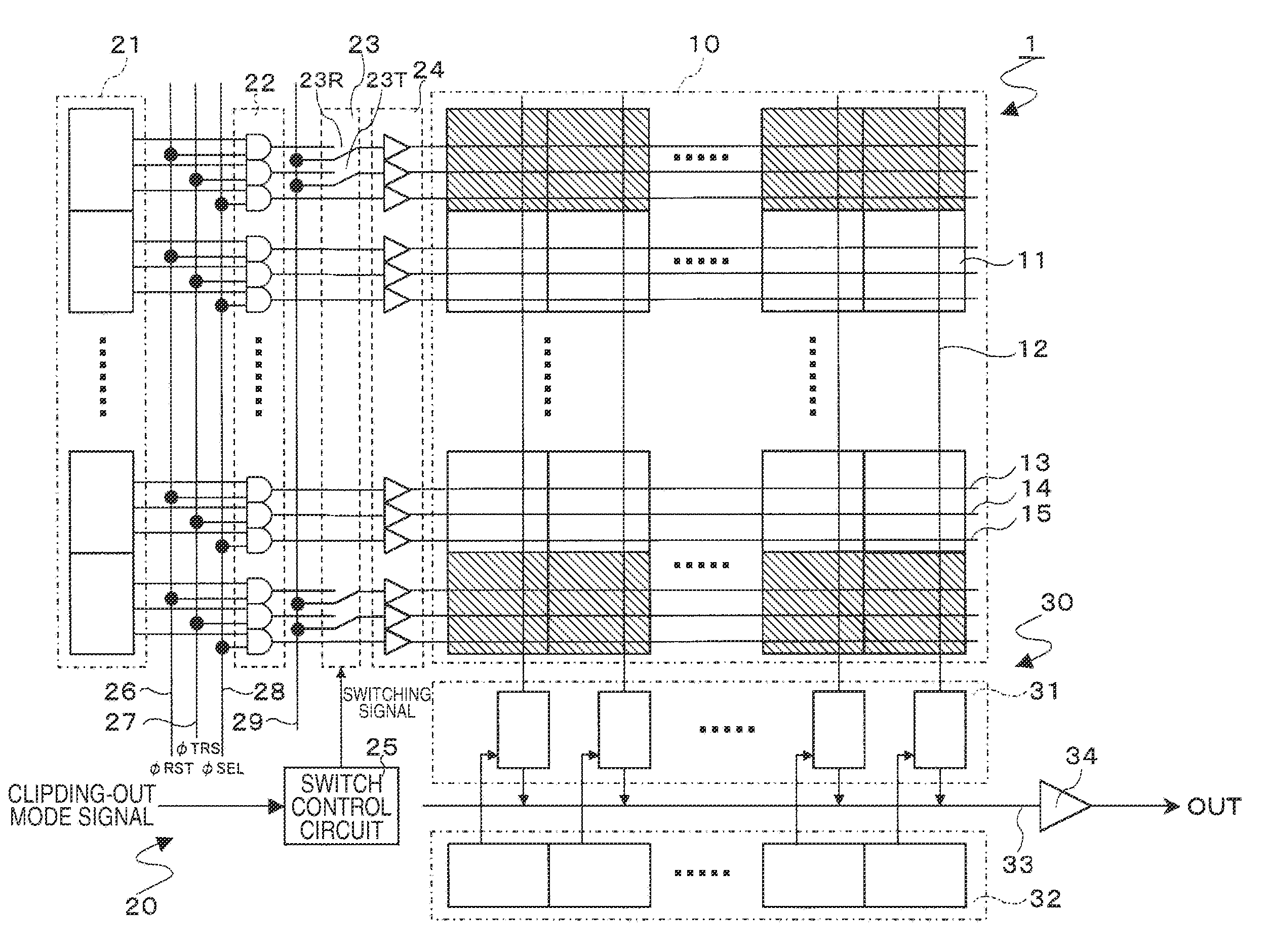
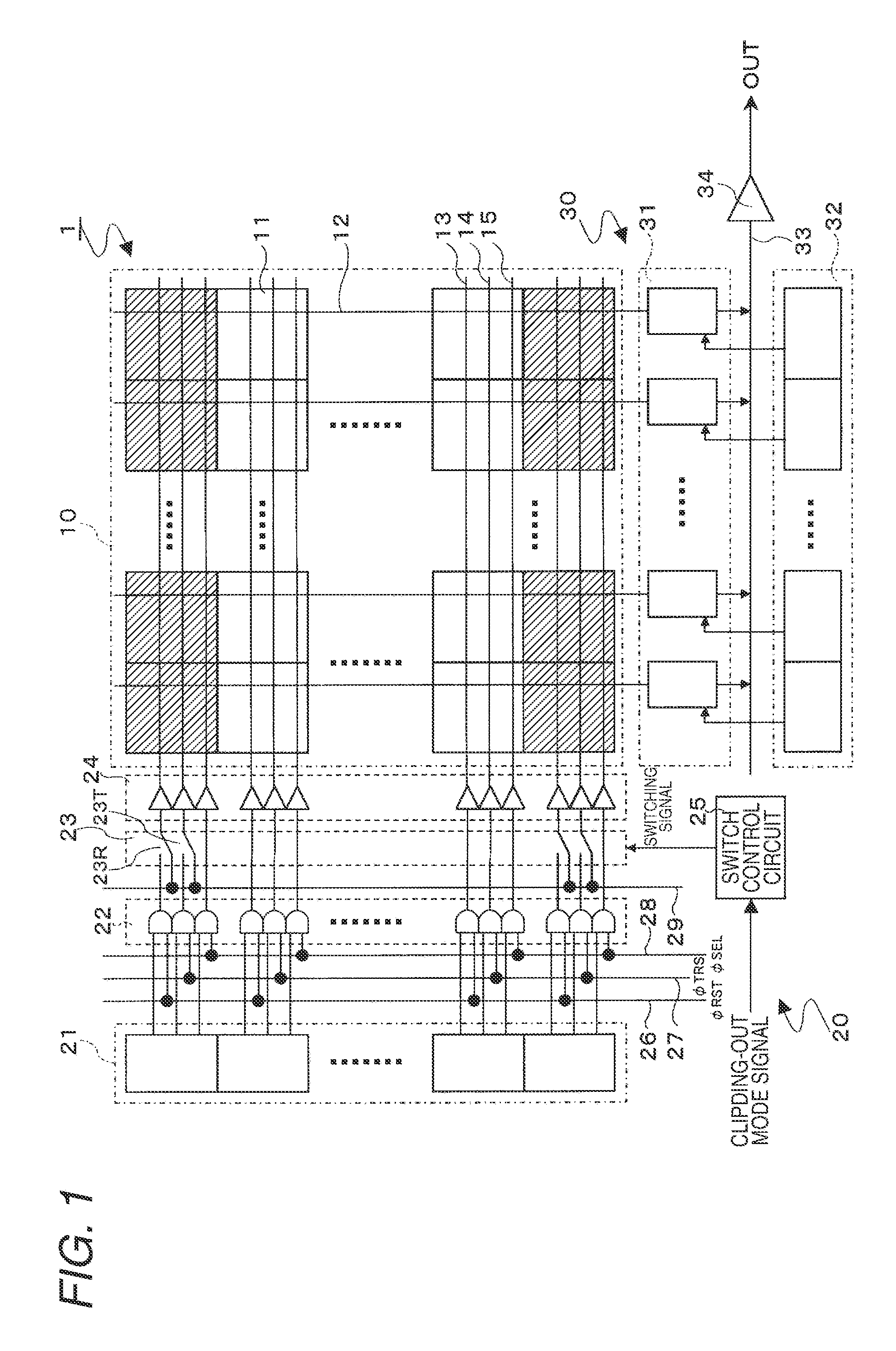
[0022]FIG. 1 is a block diagram showing an example of a constitution of a solid state imaging device, for example, a CMOS image sensor according to an embodiment of the invention. As shown in FIG. 1, a CMOS image sensor 1 according to this embodiment includes a pixel array section 10, a vertical driver 20, and a horizontal driver 30.

[0023] In the pixel array section 10, unit pixels (hereinafter simply referred to as “pixels” in some cases) 11 including photoelectric conversion elements are two-dimensionally arranged. A vertical signal line 12 is wired for each pixel column of the pixel arrangement and driving lines such as a reset line 13, a charge transfer line 14, and a selection line 15 are wired for each pixel row.

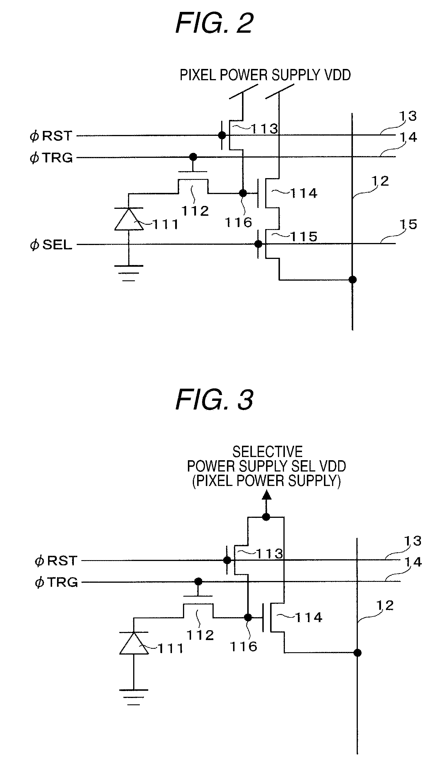
[0024]FIG. 2 is a circuit diagram showing an example of a circuit configuration of the unit pixel 11. In the figure, sections equivalent to those ...


PUM


Abstract

A solid state imaging device includes: a pixel array section in which pixels including photoelectric conversion elements are two dimensionally arranged; a vertical selector that sequentially applies selective scanning to respective rows of the pixel array section; and a controller that discharges, when a mode for reading out only pixel signals of respective rows in a given row range in the pixel array section is set by the vertical selector, charges generated in the photoelectric conversion elements in respective pixels of rows outside the row range to a pixel power supply.

Description

CROSS-REFERENCES TO RELATED APPLICATIONS [0001] This application contains subject matter related to Japanese Patent Application JP 2005-043354 filed in the Japanese Patent Office on Feb. 21, 2005, the entire contents of which being incorporated herein by reference. BACKGROUND OF THE INVENTION [0002] 1. Field of the Invention [0003] The present invention relates to a solid state imaging device, a method of driving the solid state imaging device, and an image pickup apparatus, and, more particular to a line-sequential solid state imaging device that reads out pixel signals by a unit of row according to vertical scanning, a method of driving the solid state imaging device, and an image pickup apparatus. [0004] The image pickup apparatus refers to a camera module including a solid state imaging device serving as an imaging device, an optical system for focusing image light of a subject on an imaging surface (a light-receiving surface) of the solid state imaging device, and a signal proc...

Claims


Application Information

Patent Timeline
Patent Type & Authority Applications(United States)
IPC IPC(8): H01L27/00H01L27/146H04N5/335H04N5/341H04N5/357H04N5/369H04N5/374
CPCH04N3/155H04N3/1562H04N25/445H04N25/745H04N25/75
Inventor YOKOTA, KAZUHIDEKUREBAYASHI, HISASHI
Owner SONY CORP
Why Eureka
Try Eureka