

Surface-stabilized semiconductor device
a surface stabilization and semiconductor technology, applied in the field of semiconductor devices, can solve the problems of current collapse, current leakage between electrodes, electrical instability of the semiconductor surface, etc., and achieve the effect of positive and reliable economics
- Summary
- Abstract
- Description
- Claims
- Application Information
AI Technical Summary
Benefits of technology
Problems solved by technology
Method used
Image

Examples
embodiment
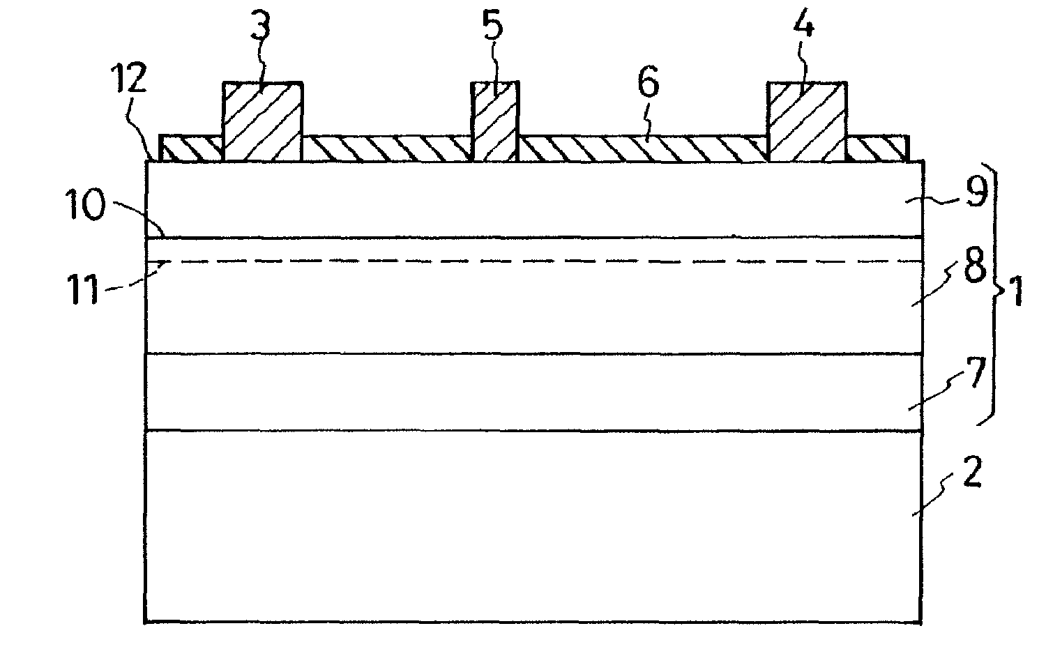
of FIG. 2
[0046]The HEMT seen here is of the same construction as that of FIG. 1 except for a p-type organic semiconductor overlay 6a which covers all of that part of the major surface 12 of the main semiconductor region 1 which lies between drain 4 and gate 5. The limited coverage of the semiconductor surface 12 by the overlay 6a is effective for restriction of the lessening of electrons, and consequent current collapse, in the underlying part of the two-dimensional electron gas layer 11.
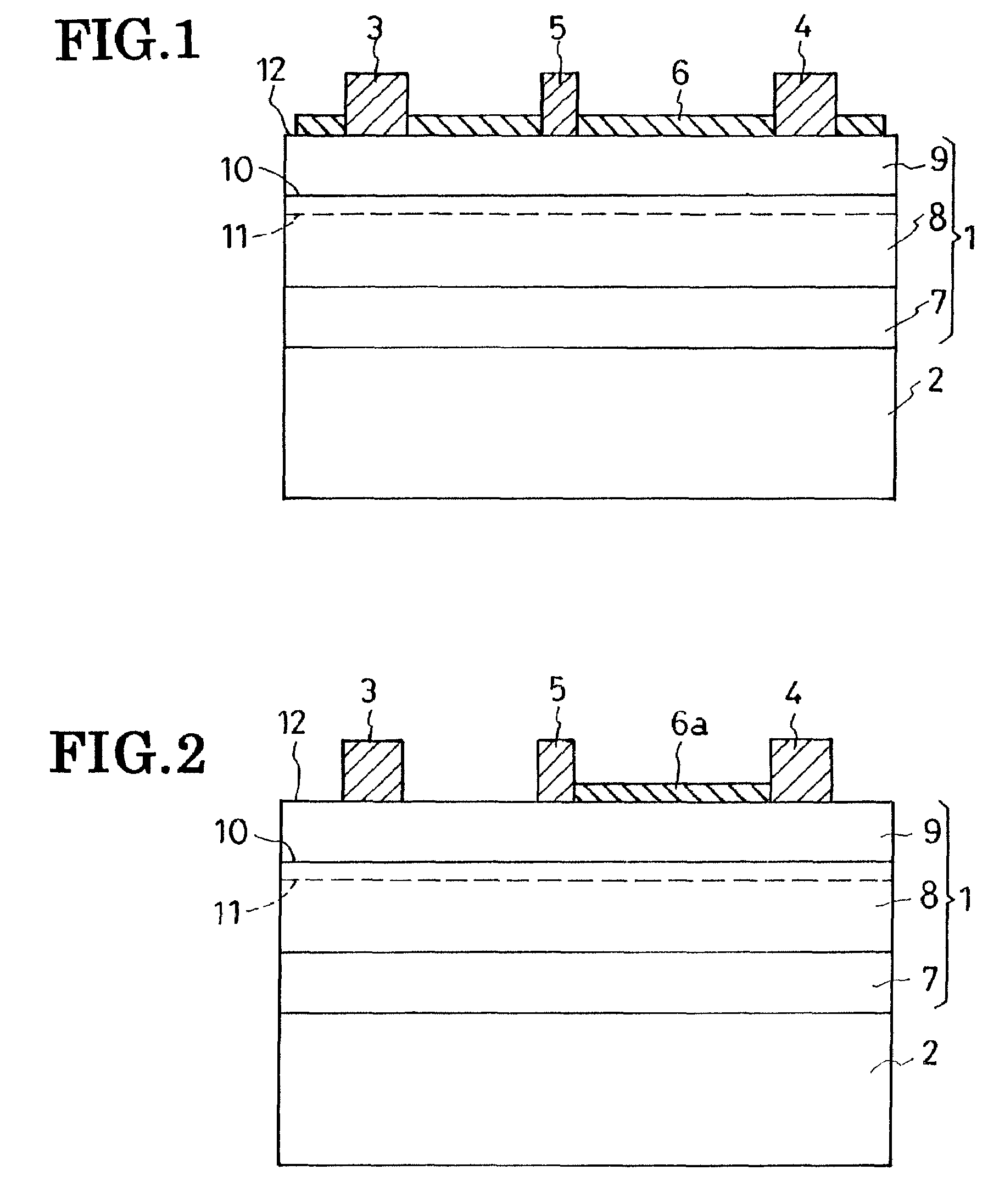
Embodiment of FIG. 3
[0047]This embodiment differs from that of FIG. 2 only in an organic semiconductor overlay 6b which covers only part of that part of the major surface 12 of the main semiconductor region 1 which lies between drain 4 and gate 5. A spacing exists between gate 5 and overlay 6b. This overlay 6b is nearly as effective as its FIG. 2 counterpart 6a.
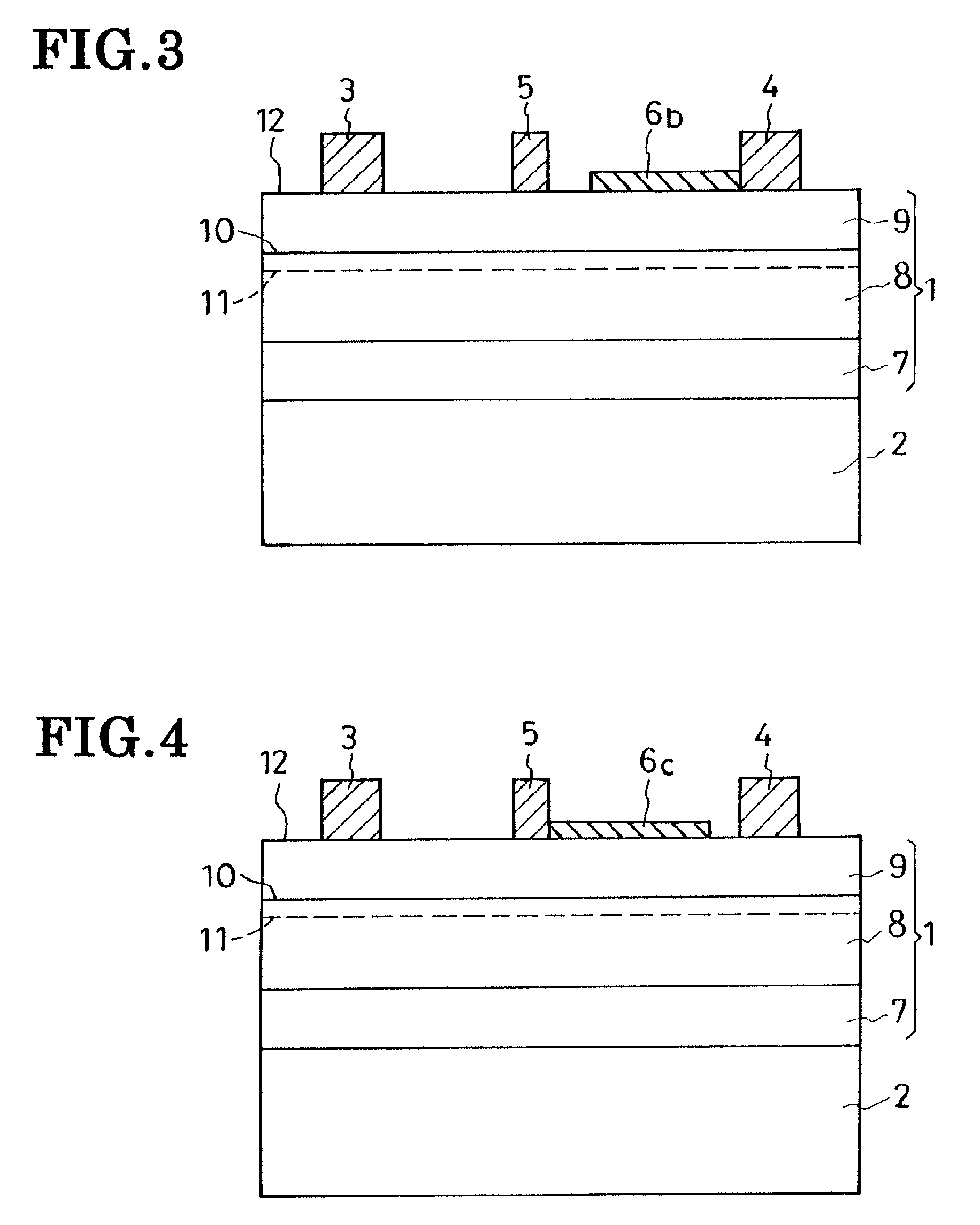
Embodiment of FIG. 4
[0048]The organic semiconductor overlay 6c depicted here is similar in size and positioning to its FIG. 3 counterpart 6b...
PUM
 Abstract
Description
Claims
Application Information