
Current control circuit with limiter, temperature control circuit, and brightness control circuit

a limiter and current control technology, applied in the direction of limiting amplitude without controlling loop, process and machine control, instruments, etc., can solve the problems of reducing size and cost, variating limiter voltage, etc., and achieve the effect of simple structur

Inactive Publication Date: 2006-08-24
NEC CORP
View PDF3 Cites 1 Cited by
  • Summary
  • Abstract
  • Description
  • Claims
  • Application Information

AI Technical Summary

Benefits of technology

The present invention provides a current control circuit with limiter that has a simple structure and removes temperature dependence of the limiter voltage while maintaining a linear and high-precision control characteristic. The current control circuit with limiter can be used in a temperature control circuit and a brightness control circuit. The technical effects of the invention include a reduction in complexity and improved control accuracy.

Problems solved by technology

The above-mentioned circuit shown in FIG. 15 has a disadvantage that a limiter voltage is varied due to a variation in Vbe of transistor 7, which is caused by temperature.
Therefore, there is a problem with respect to reductions in size and cost.

Method used


Image

  • Current control circuit with limiter, temperature control circuit, and brightness control circuit
  • Current control circuit with limiter, temperature control circuit, and brightness control circuit
  • Current control circuit with limiter, temperature control circuit, and brightness control circuit

Examples


first exemplary embodiment

1. First Exemplary Embodiment

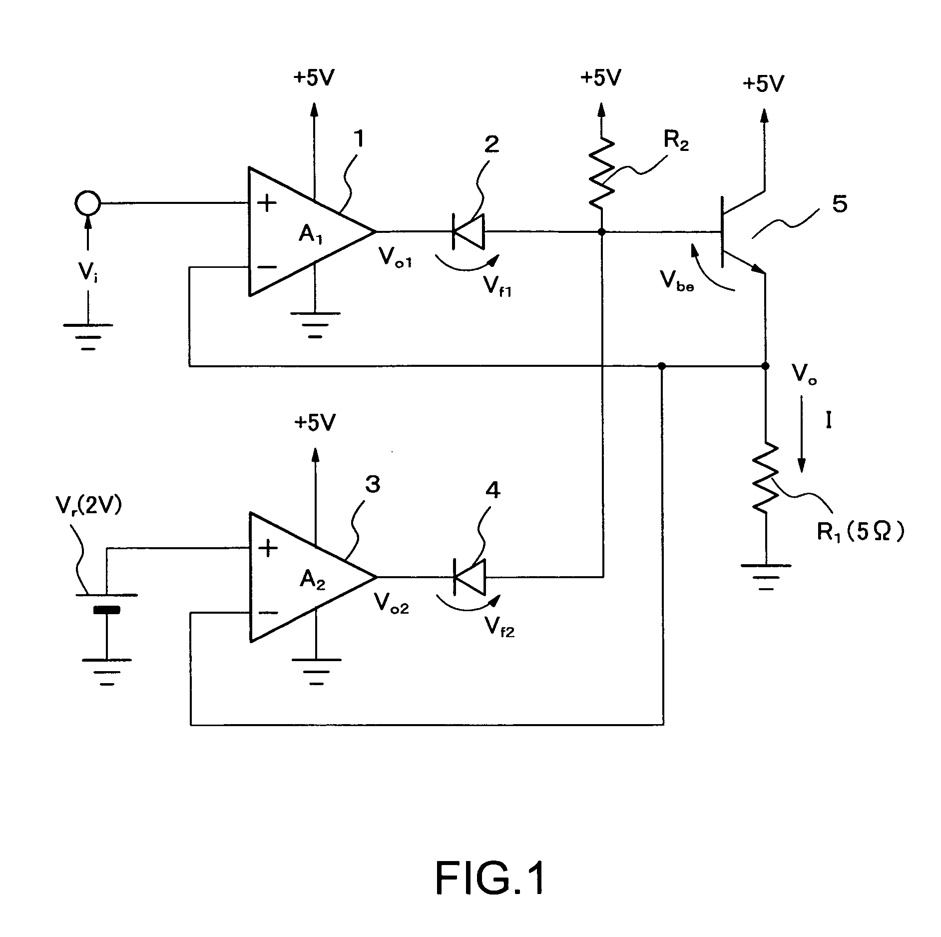
[0041] Embodiments of the present invention will be described with reference to the drawings. In each of the following embodiments, assume that an Op-Amp is an ideal Op-Amp, a voltage gain is sufficiently large, and each of an input offset voltage and an input bias current is sufficiently small and thus can be neglected. Although a power source voltage is set to +5 V, the present invention is not particularly limited to this voltage. Although a reference voltage Vr set as a limiter voltage is 2 V, Vr can be set to an arbitrary voltage within the power source voltage range of the Op-Amp. The same arbitrary setting can similarly be made in each of the following embodiments.

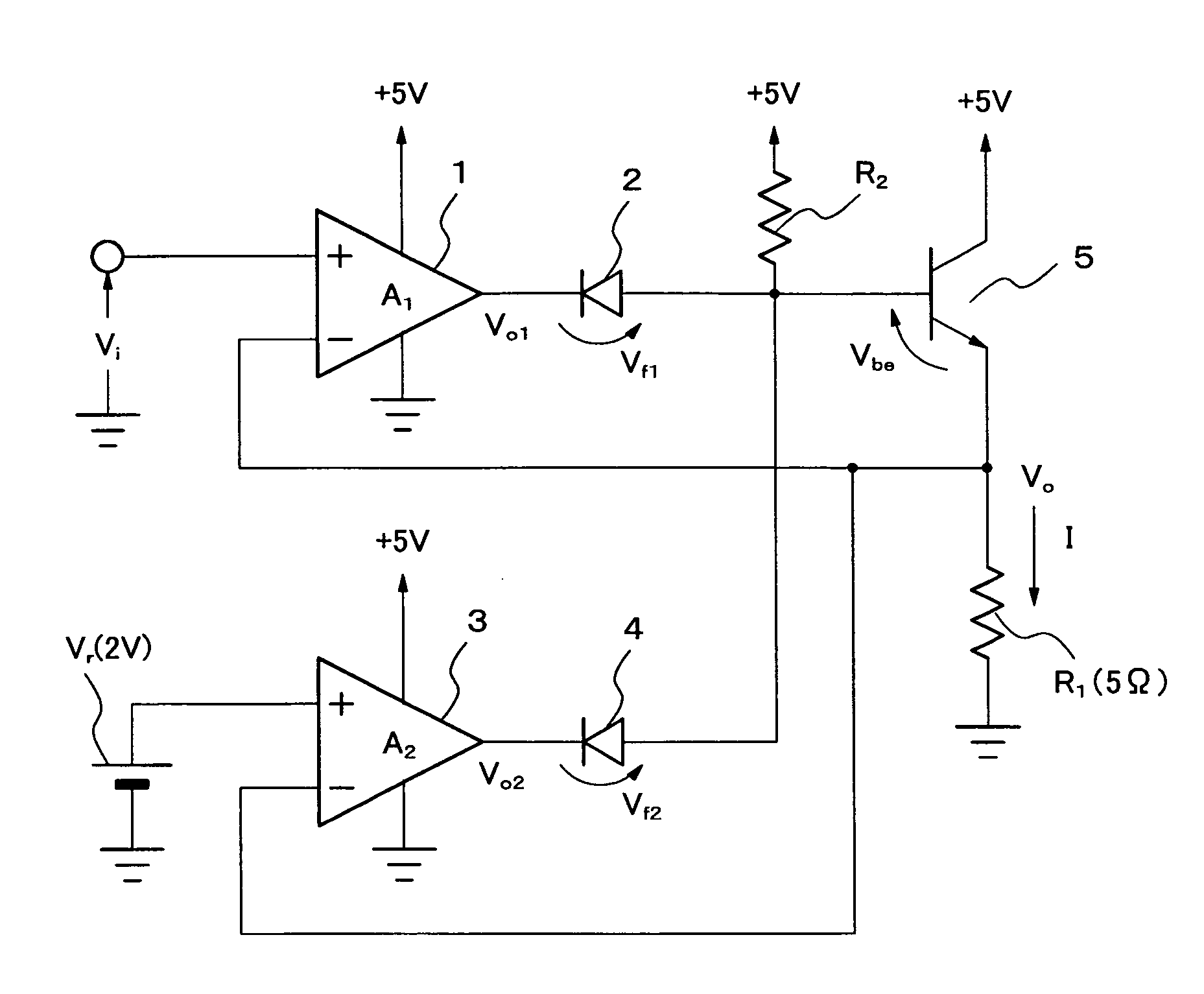
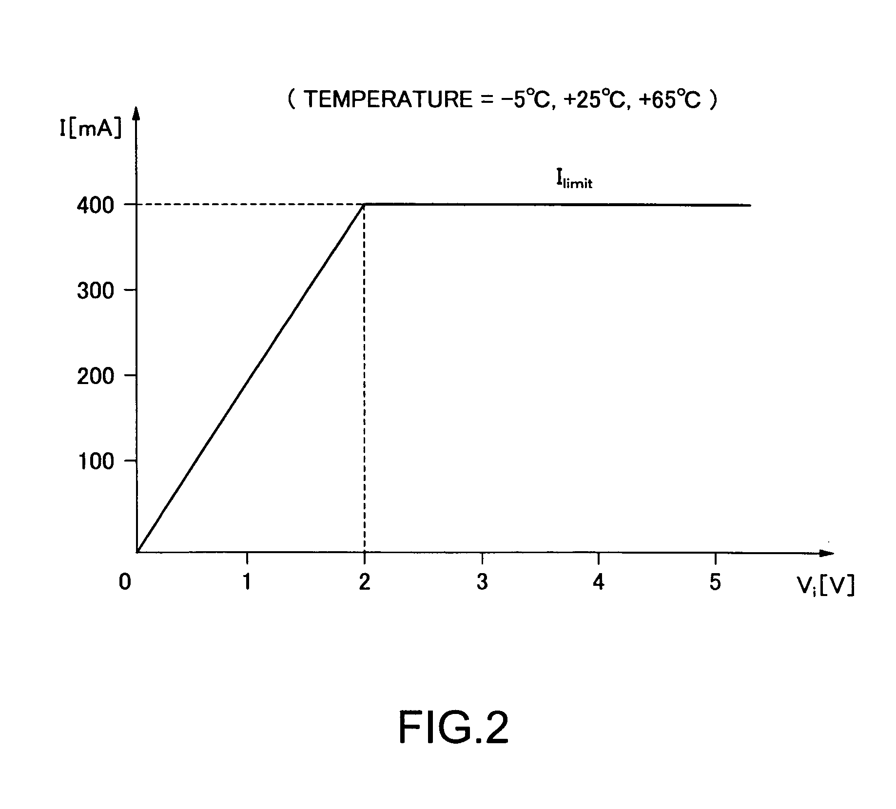
[0042]FIG. 1 is a circuit diagram showing a first embodiment of the present invention. A control input voltage Vi is connected to the non-inverting input of an Op-Amp 1. The output of the Op-Amp 1 is connected through diode 2 to the base input of an NPN transistor 5 composing the emitte...

second exemplary embodiment

2. Second exemplary Embodiment

[0067] In the first embodiment, the emitter follower is composed of the NPN transistor 5. The emitter follower can be composed of a PNP transistor. The transistor to be used is not limited to a bipolar transistor. It is apparent that a source follower composed of a field effect transistor including a MOS transistor may be used. At this time, the channel type of the field effect transistor may be an N-channel type or a P-channel type.

[0068] Next, an exemplary embodiment of the present invention in a case where the NPN transistor 5 is replaced by another type of transistor will be described.

[0069]FIG. 3 is a circuit diagram showing a second exemplary embodiment of the present invention. The NPN transistor 5 shown in FIG. 1 is replaced by an n-channel field effect transistor 8. The operation of a circuit according to the second embodiment will be described with reference to FIG. 3 and numerical expressions.

[0070] First, the operation of Op-Amp 1 will be...

third exemplary embodiment

3. Third exemplary Embodiment

[0080]FIG. 4 is a circuit diagram showing a third exemplary embodiment of the present invention. The NPN transistor 5 shown in FIG. 1 is replaced by a PNP transistor 9. In the third exemplary embodiment, the connection direction of each of diode 2 and diode 4 is reversed to that in each of the first exemplary embodiment and the second exemplary embodiment. That is, the anode of diode 2 is connected with the output terminal of Op-Amp 1 and the cathode thereof is connected with the base of the PNP transistor 9. The anode of diode 4 is connected with the output terminal of the Op-Amp 3 and the cathode thereof is connected with the base of PNP transistor 9.

[0081] In the circuit shown in FIG. 4, when Vi is higher than Vr, diode 4 subjected to wired OR connection goes into the Off-state. Therefore, the feedback circuit of Op-Amp 3 is interrupted and the output thereof is blocked. On the other hand, because diode 2 goes into the On-state, negative feedback is ...


PUM


Abstract

A current control circuit with limiter includes a voltage follower as the output unit of the current control circuit, the voltage follower including a transistor, the circuit further including two operational amplifiers and two diodes. In a first operational amplifier, the non-inverting input receives an input voltage to the current control circuit and the inverting input receives the output of the voltage follower. In a second operational amplifier, the non-inverting input receives a predetermined voltage and the inverting input receives the output of the voltage follower. A first diode is connected between the output of the first operational amplifier and the input of the voltage follower. A second diode is connected between the output of the second operational amplifier and the input of the voltage follower.

Description

BACKGROUND OF THE INVENTION [0001] 1. Field of the Invention [0002] The present invention relates to a current control circuit with limiter, and more particularly, to a current control circuit with limiter for generating a current proportional to an input voltage when the input voltage is smaller than a predetermined voltage and generating a constant current when the input voltage is equal to or higher than the predetermined voltage. The present invention also relates to a temperature control circuit using the current control circuit with limiter and a brightness control circuit using the current control circuit with limiter. [0003] 2. Description of the Related Art [0004]FIG. 15 shows a conventional example of a current control circuit with limiter. A control input voltage Vi is applied to the non-inverting input terminal of an operational amplifier (hereinafter referred to as “OP-Amp”) 1 which operates as a voltage follower. The output of Op-Amp 1 is connected to the non-inverting...

Claims


Application Information

Patent Timeline
Patent Type & Authority Applications(United States)
IPC IPC(8): G05F1/40
CPCG05F1/56H03G11/002
Inventor YOSHIZAWA, NOBUKAZU
Owner NEC CORP
Learn More