Waveguide type optical device
a waveguide and optical device technology, applied in optics, optical light guides, instruments, etc., can solve the problems of large size increased cost of arrayed waveguide grating optical multiplexer/demultiplexer, and so as to reduce the influence of pdl and eliminate temperature dependence and polarization dependen
- Summary
- Abstract
- Description
- Claims
- Application Information
AI Technical Summary
Benefits of technology
Problems solved by technology
Method used
Image
Examples
first embodiment
[0073]In the following, a mode for carrying out the present invention is described with reference to a drawing. FIG. 6 shows the structure of an arrayed waveguide grating optical multiplexer / demultiplexer 106 of this embodiment. This embodiment is characterized in that a polarization dependence eliminating means inserted to the arrayed waveguide eliminates the polarization dependence due to birefringence of the arrayed waveguide and a temperature-dependence compensator. In the following, this structure is described in detail with reference to the drawing.
[0074]FIG. 6 is a schematic view of the arrayed waveguide grating optical multiplexer / demultiplexer 106. As shown in FIG. 6, the arrayed waveguide grating optical multiplexer / demultiplexer 106 is formed with a silica-based waveguide on a waveguide substrate 11 that is made of silicon. The silica-based waveguide includes: at least one input channel waveguide 13 that is connected to an input port 12; an input slab waveguide 14 that is...
second embodiment
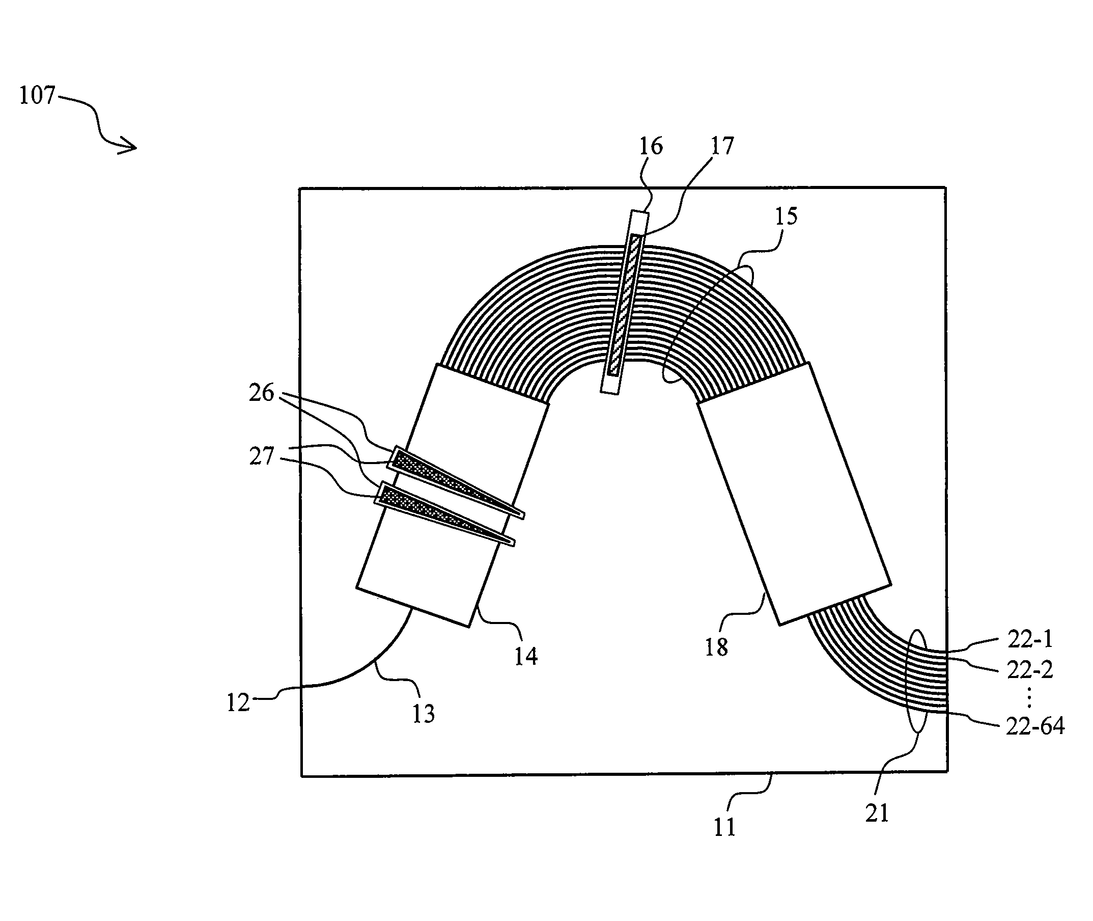
[0083]FIG. 7 is a schematic view of an arrayed waveguide grating optical multiplexer / demultiplexer 107. The difference between the arrayed waveguide grating optical multiplexer / demultiplexer 107 and the arrayed waveguide grating optical multiplexer / demultiplexer 106 of FIG. 6 is that the temperature-dependence compensator 27 is placed on the input slab waveguide 14, instead of the arrayed waveguide 15. Alternatively, the temperature compensating means 27 may be placed on the output slab waveguide 18, instead of the input slab waveguide 14.
[0084]The arrayed waveguide grating optical multiplexer / demultiplexer 107 has two grooves 26 extending across the input slab waveguide 14. The number of grooves 26 is not limited to two. The grooves 26 are designed to have smaller width on the inner side of the curved arrayed waveguide 15, and have greater width on the outer side. The temperature compensating means 27 is inserted into the grooves 26, as in the arrayed waveguide grating optical mult...
third embodiment
[0088]FIG. 9 is a schematic view of an arrayed waveguide grating optical multiplexer / demultiplexer 109. The differences between the arrayed waveguide grating optical multiplexer / demultiplexer 109 and the arrayed waveguide grating optical multiplexer / demultiplexer 107 of FIG. 7 are that the polarization dependence eliminating means 17 is not obliquely placed, and is not located at the center of the arrayed waveguide 15. There is a polarization dependence distribution of refractive index at the straight-line portion 15a, and the differences in refractive index among the waveguides have the polarization dependence. More specifically, the channel waveguide pitch is narrower on the shorter waveguide side of the arrayed waveguide 15, and the channel waveguide pitch is wider on the longer waveguide side of the arrayed waveguide 15. For example, the number of waveguides in the arrayed waveguide 15 is 250, the minimum pitch of the channel waveguides of the arrayed waveguide 15 is 15 μm, and ...
PUM
 Abstract
Description
Claims
Application Information


