Method of forming isolated features of semiconductor devices

a technology of semiconductor devices and isolated features, which is applied in the manufacturing of semiconductor/solid-state devices, basic electric elements, electric devices, etc., can solve the problem of becoming more difficult to pattern material layers, and achieve the effect of small pitch and sharp resolution

Active Publication Date: 2006-08-24
INFINEON TECH AG
View PDF4 Cites 9 Cited by
  • Summary
  • Abstract
  • Description
  • Claims
  • Application Information

AI Technical Summary

Benefits of technology

[0010] Advantages of preferred embodiments of the present invention include providing an improved method of accurately patterning dense isolated regions of small features. Ultra-dense features having a small pitch and sharp resolution that are isolated or formed in isolated groups may be manufactured using the method described herein.

Problems solved by technology

However, as semiconductor devices become smaller, it becomes more difficult to pattern material layers because of diffraction and other effects that occur during the lithography process.

Method used


Image

  • Method of forming isolated features of semiconductor devices
  • Method of forming isolated features of semiconductor devices
  • Method of forming isolated features of semiconductor devices

Examples


Embodiment Construction

[0023] The making and using of the presently preferred embodiments are discussed in detail below. It should be appreciated, however, that the present invention provides many applicable inventive concepts that can be embodied in a wide variety of specific contexts. The specific embodiments discussed are merely illustrative of specific ways to make and use the invention, and do not limit the scope of the invention.

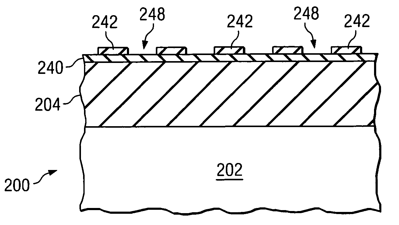
[0024] The present invention will be described with respect to preferred embodiments in a specific context, namely a method of patterning isolated contact holes of semiconductor devices. The invention may also be applied, however, to the patterning of other relatively isolated features or groups of features of semiconductor devices, such as patterns for features comprising a minimum feature size of the device, resistor islands, or relatively short conductive lines, as examples.

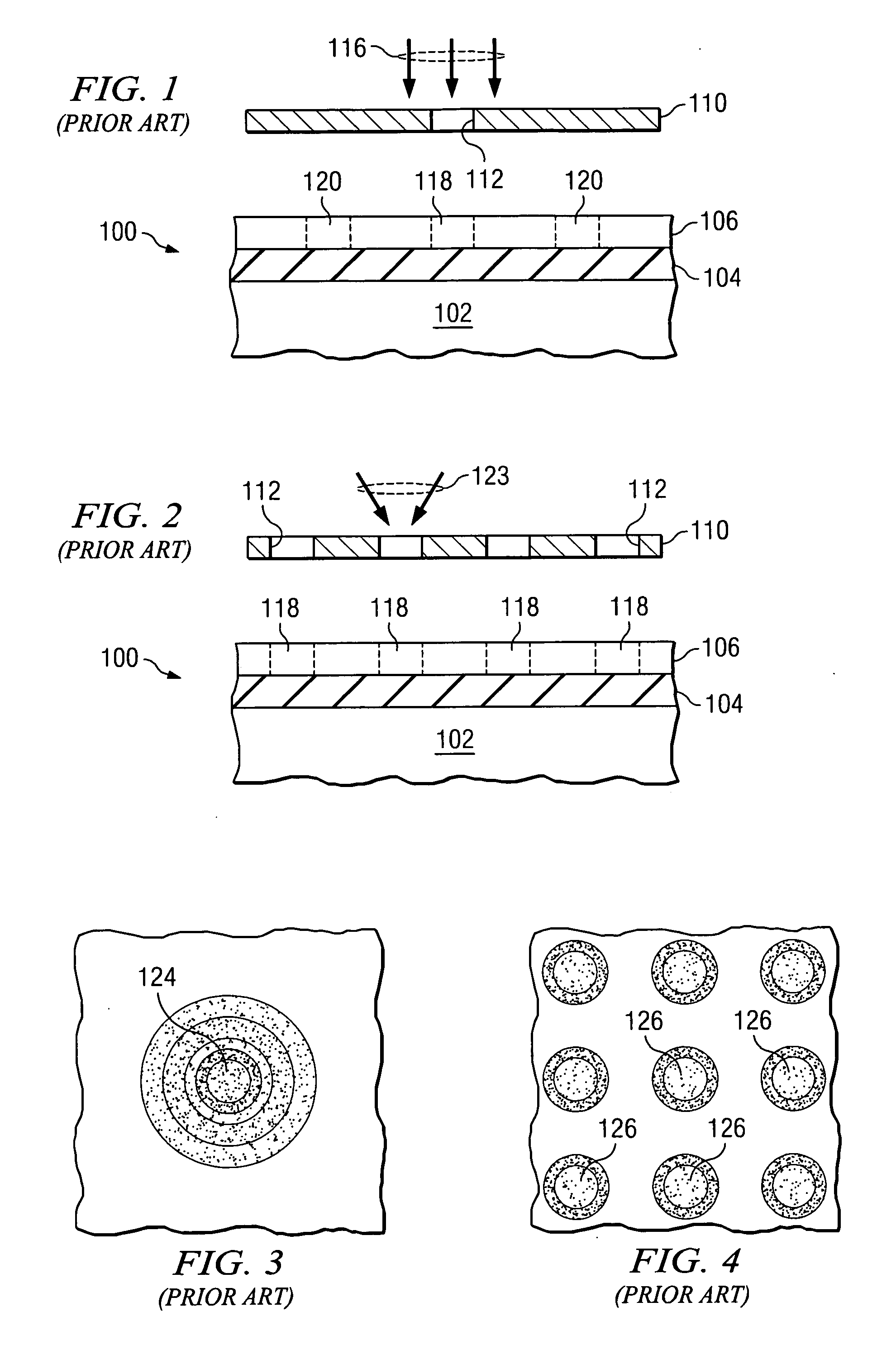
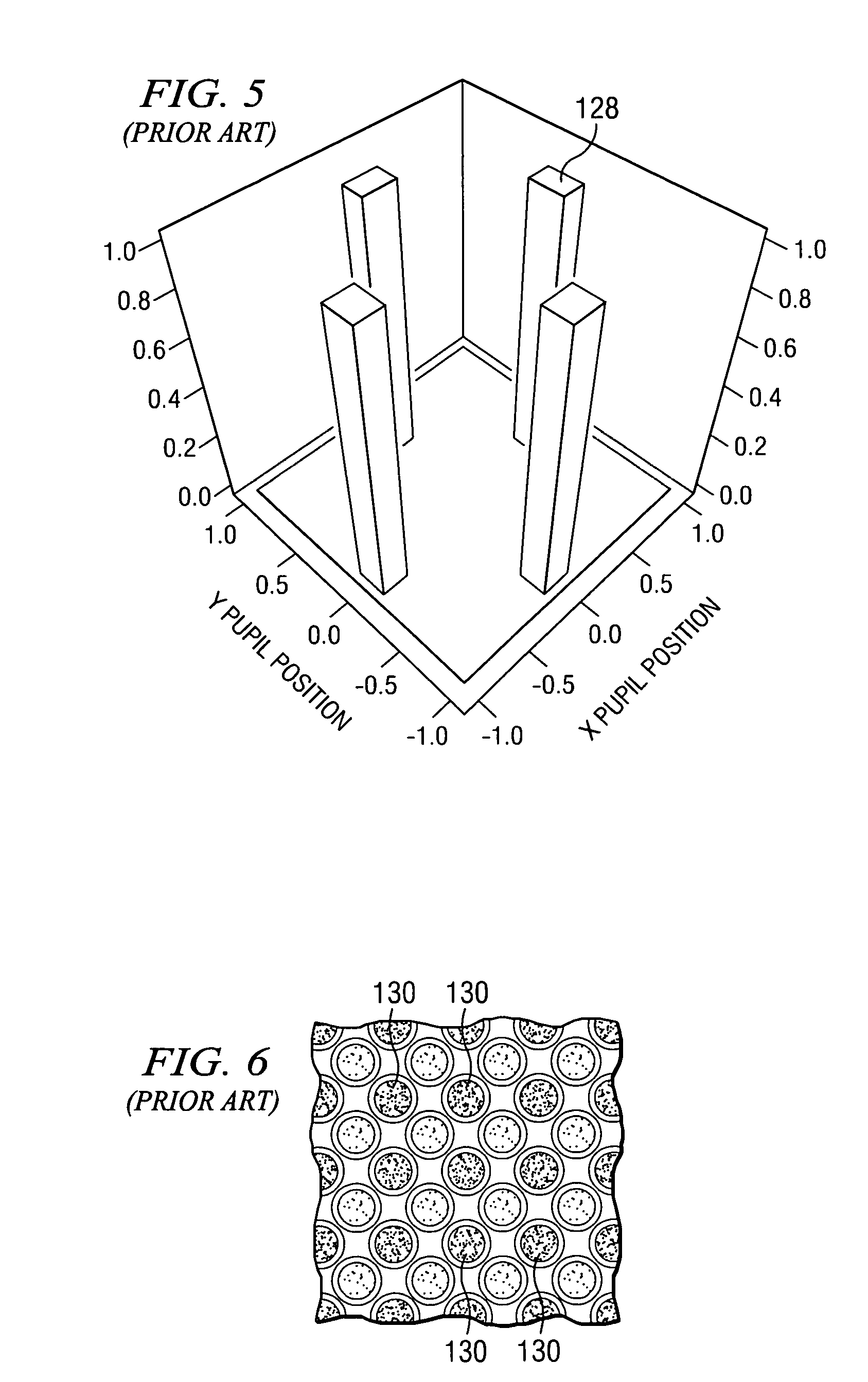
[0025] Prior art lithography techniques will first be discussed, with reference to FIGS. 1 throug...


PUM

PropertyMeasurementUnit
widthaaaaaaaaaa
widthaaaaaaaaaa
thicknessaaaaaaaaaa

Abstract

A method of forming isolated features of semiconductor devices is disclosed. A first hard mask is deposited over a material layer to be patterned, and a second hard mask is deposited over the first hard mask. The second hard mask is patterned with a pattern for an array of features using an off-axis lithography method. A portion of the pattern for the array of features is transferred to the first hard mask. The first hard mask is then used as a mask to pattern the material layer.

Description

TECHNICAL FIELD [0001] The present invention relates generally to the fabrication of semiconductor devices, and more particularly to the formation of isolated features of integrated circuits. BACKGROUND [0002] Semiconductor devices are used in a variety of electronic applications, such as computers, cellular phones, personal computing devices, and many other applications. Home, industrial, and automotive devices that in the past comprised only mechanical components now have electronic parts that require semiconductor devices, for example. [0003] Semiconductor devices are manufactured by depositing many different types of material layers over a semiconductor workpiece or wafer, and patterning the various material layers using lithography. The material layers typically comprise thin films of conductive, semiconductive, and insulating materials that are patterned and etched to form integrated circuits (IC's). There may be a plurality of transistors, memory devices, switches, conductive...

Claims


Application Information

Patent Timeline
Patent Type & Authority Applications(United States)
IPC IPC(8): H01L21/4763
CPCH01L21/0332H01L21/0337H01L21/76838H01L21/76816
Inventor SCHROEDER, UWE PAUL
Owner INFINEON TECH AG
Why Eureka
Try Eureka