NAND-type non-volatile memory cell and method for operating same

a non-volatile memory cell, non-volatile technology, applied in the direction of digital storage, instruments, semiconductor devices, etc., can solve the problems of negative charge accumulation, nand arrays require more semiconductor real estate, and breakage in the insulating material, etc., to achieve low power required to program or erase memory cells, simple fabrication of nand arrays, and high density

Active Publication Date: 2006-02-07
MACRONIX INT CO LTD
View PDF13 Cites 62 Cited by
  • Summary
  • Abstract
  • Description
  • Claims
  • Application Information

AI Technical Summary

Benefits of technology

[0016]The present invention addresses these needs by providing non-volatile flash memory capable of storing two bits per cell in a NAND array. The fabrication of the NAND array is simple, and the power required to program or erase memory cells is low. The NAND array of the present invention further provides for high density and small pitch in the design.

Problems solved by technology

This causes a breakdown in the insulating material and allows a negative charge to accumulate on the floating gate.
However, NOR arrays require more semiconductor real estate than do NAND arrays.
Besides, NAND memory cells utilizing floating gates still need complex fabricating process and design circuits.

Method used


Image

  • NAND-type non-volatile memory cell and method for operating same
  • NAND-type non-volatile memory cell and method for operating same
  • NAND-type non-volatile memory cell and method for operating same

Examples


Embodiment Construction

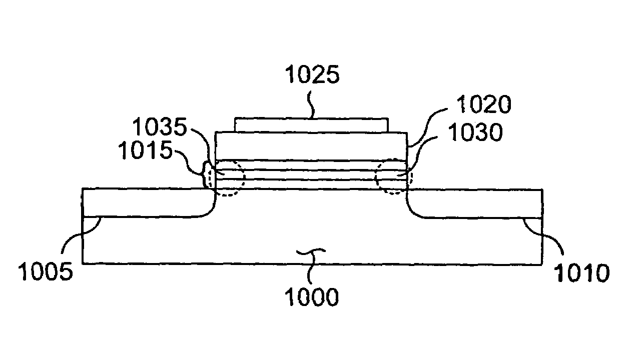
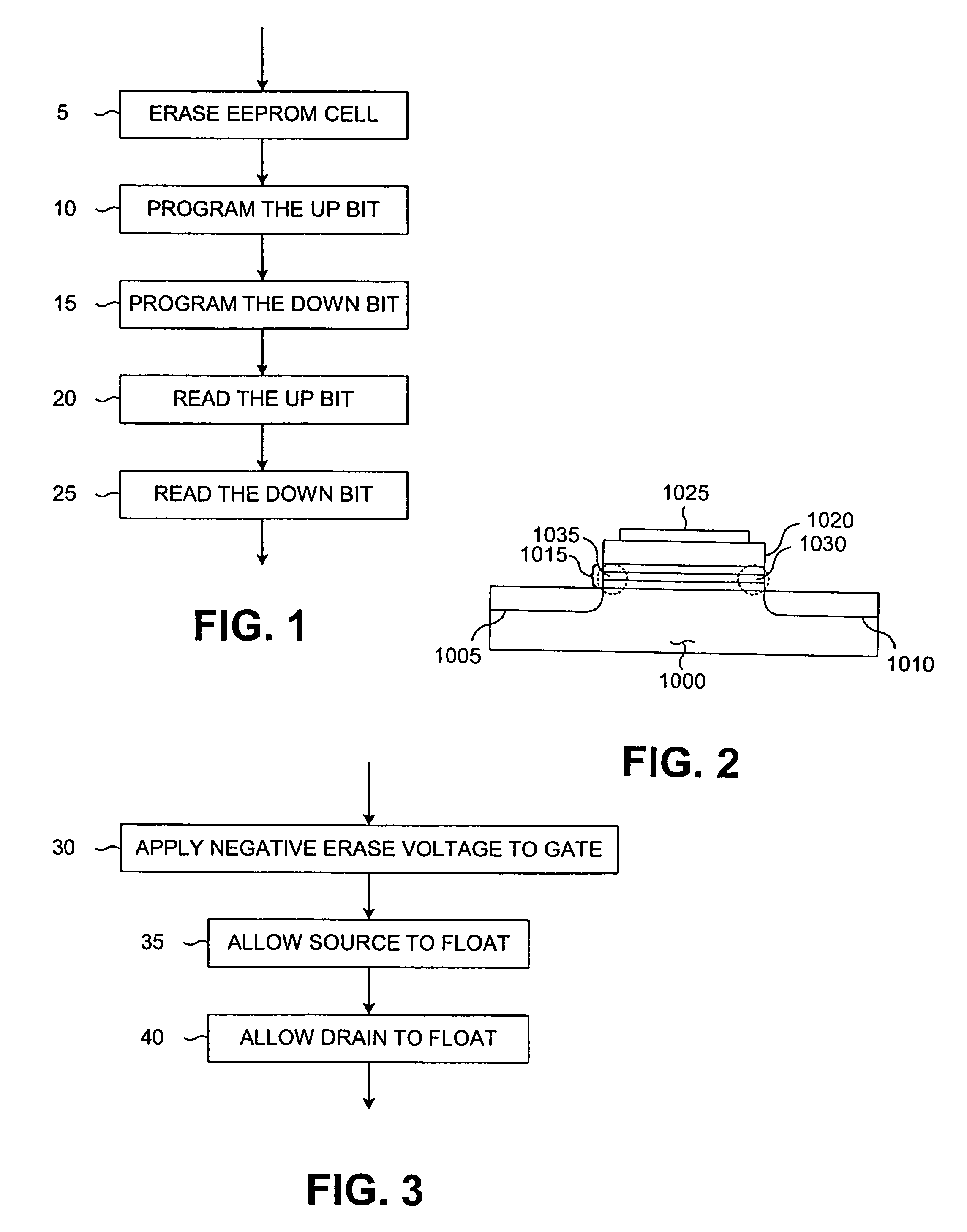
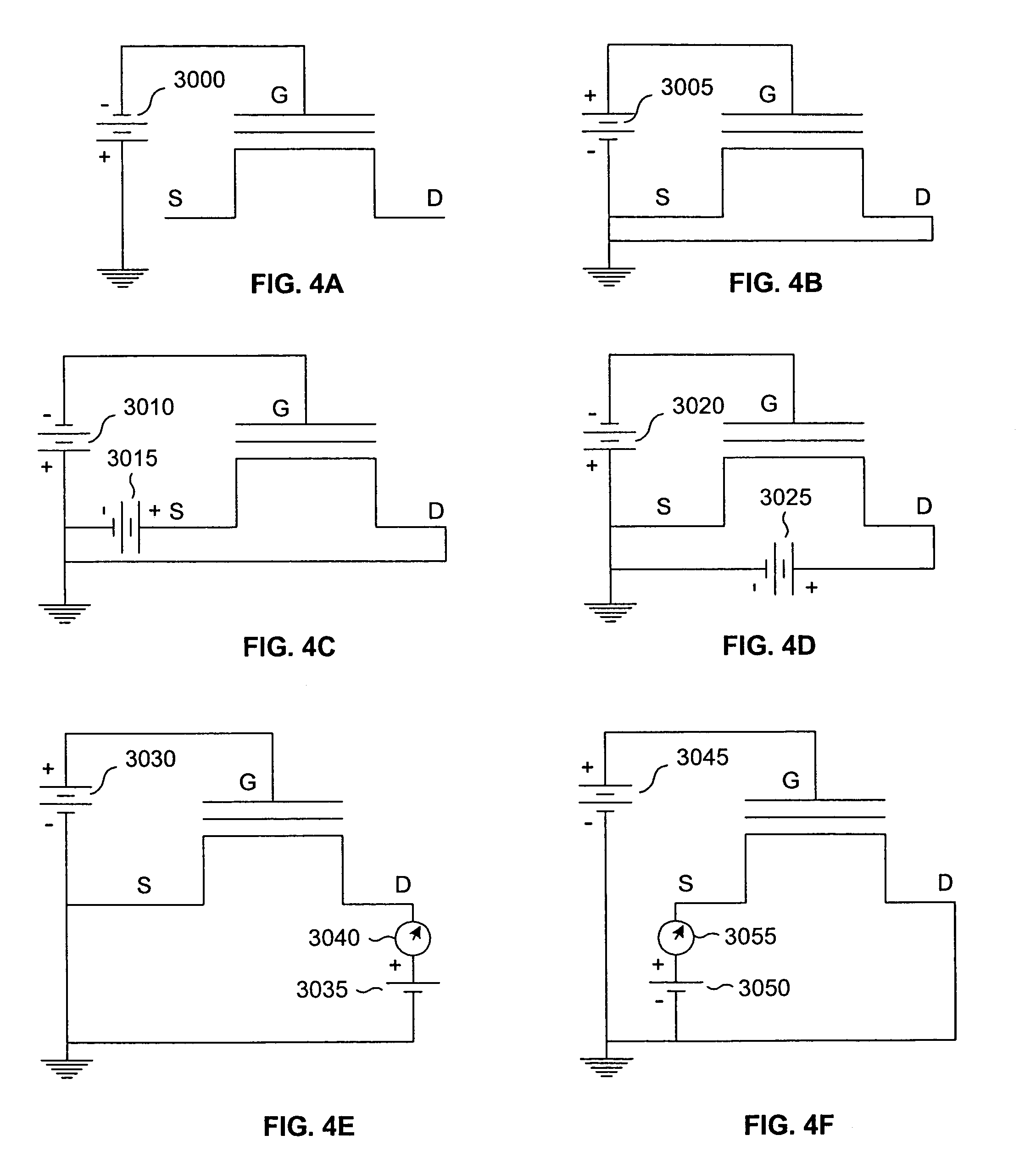
[0052]Reference will now be made in detail to the presently preferred embodiments of the invention, examples of which are illustrated in the accompanying drawings. Wherever possible, the same or similar reference numbers are used in the drawings and the description to refer to the same or like parts. It should be noted that the drawings are in simplified form and are not to precise scale. In reference to the disclosure herein, for purposes of convenience and clarity only, directional terms, such as, top, bottom, left, right, up, down, over, above, below, beneath, rear, and front, are used with respect to the accompanying drawings. Such directional terms should not be construed to limit the scope of the invention in any manner.

[0053]Although the disclosure herein refers to certain illustrated embodiments, it is to be understood that these embodiments are presented by way of example and not by way of limitation. The intent of the following detailed description, although discussing exe...


PUM


Abstract

A NAND-type erasable programmable read only memory (EEPROM) device formed of a number of substantially identical EEPROM cells with each EEPROM cell being capable of storing two bits of information. A simple method for operating the memory comprises erasing, programming, and reading the device.

Description

[0001]This application claims the benefit of foreign priority under 35 U.S.C. Section 119 of European Patent Application No. 03022518.9, filed on Oct. 2, 2003, the contents of which are incorporated herein by reference.BACKGROUND OF THE INVENTION[0002]1. Field of the Invention[0003]The present invention relates generally to non-volatile memory devices and, more particularly, to methods of operating localized trapped charge memory cell structures capable of storing multiple bits per cell.[0004]2. Description of Related Art[0005]A non-volatile semiconductor memory device is designed to maintain programmed information even in the absence of electrical power. Read only memory (ROM) is a non-volatile memory commonly used in electronic equipment such as microprocessor-based digital electronic equipment and portable electronic devices.[0006]ROM devices typically include multiple memory cell arrays. Each memory cell array may be visualized as including intersecting word lines and bit lines....

Claims


Application Information

Patent Timeline
Patent Type & Authority Patents(United States)
IPC IPC(8): G11C11/34G11C16/04G11C16/10H01L27/115
CPCG11C16/0475H01L27/115G11C16/10H10B69/00
Inventor YEH, CHIH CHIEHTSAI, WEN JERLU, TAO CHENG
Owner MACRONIX INT CO LTD
Why Eureka
Try Eureka