Solid-state imaging device

Active Publication Date: 2006-08-31
COLLABO INNOVATIONS INC
View PDF11 Cites 17 Cited by
  • Summary
  • Abstract
  • Description
  • Claims
  • Application Information

AI Technical Summary

Benefits of technology

[0013] Therefore, an object of the present invention is to clarify a new circuit configuration of a sensor in

Problems solved by technology

However, as for a sensor in which photosensitive cells are each formed by three transis

Method used


Image

  • Solid-state imaging device
  • Solid-state imaging device
  • Solid-state imaging device

Examples


Example

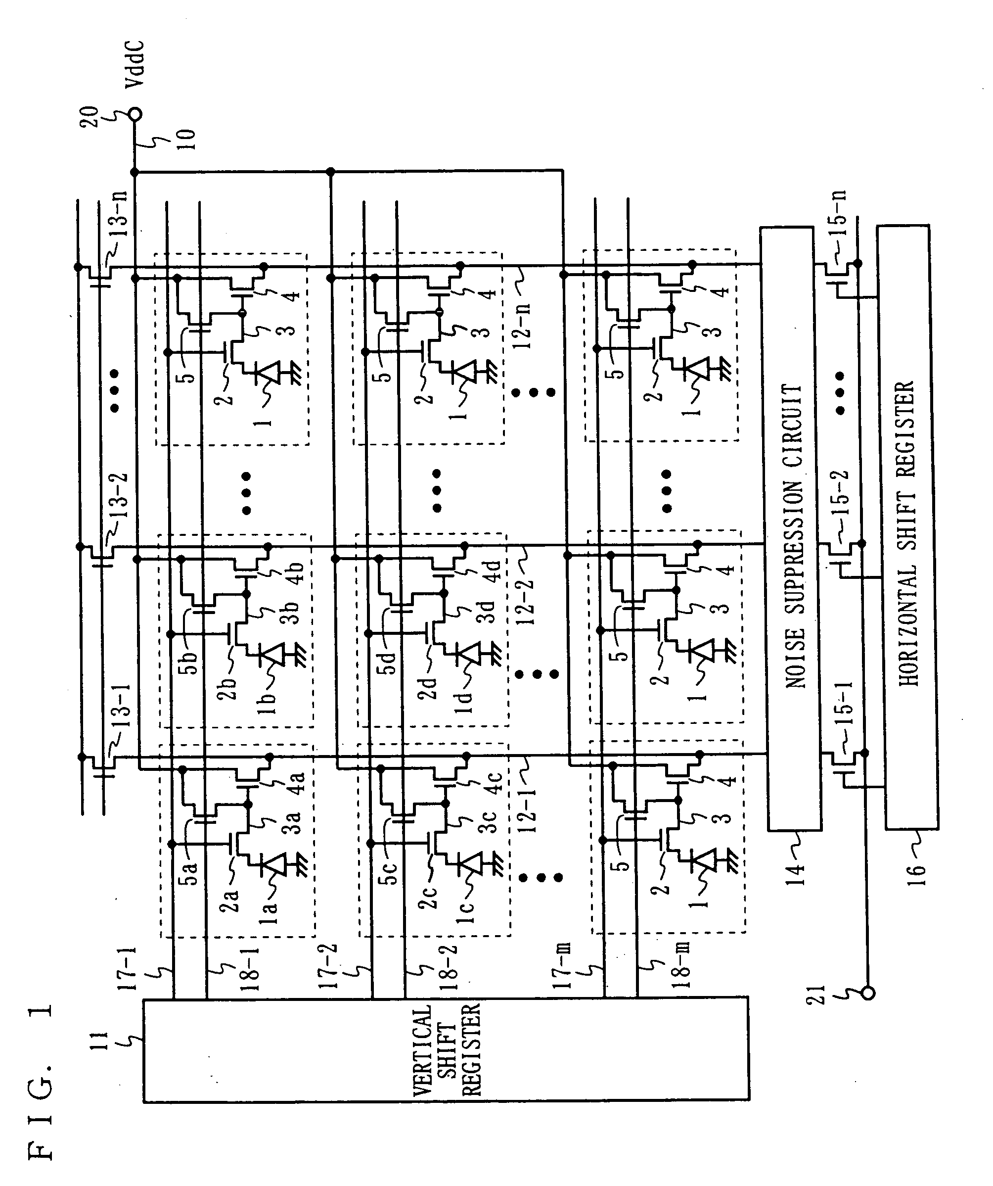
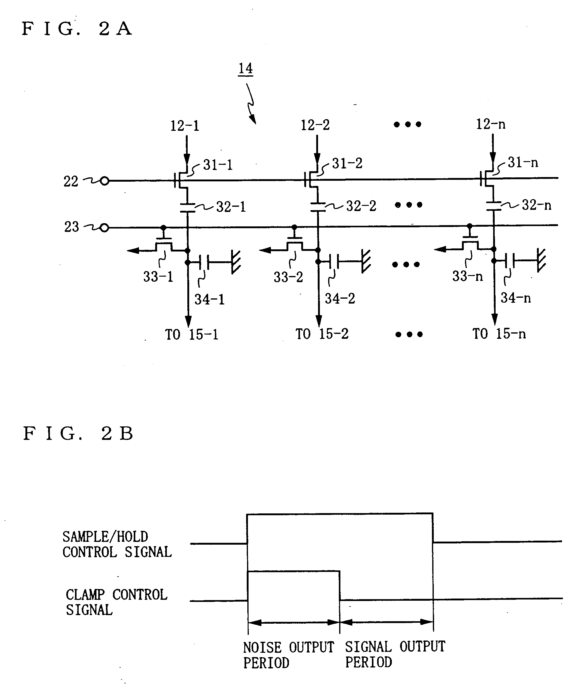
[0037] Prior to descriptions of a sensor according to an embodiment of the present invention, an exemplary sensor in which photosensitive cells are each formed by three transistors is described. The exemplary sensor illustrated in FIG. 1 includes photosensitive cells (each surrounded by a dotted line) arranged in an m×n matrix, a power supply line 10, a vertical shift register 11, n vertical signal lines 12-1 through 12-n, n load registers 13-1 through 13-n, a noise suppression circuit 14, n horizontal transistors 15-1 through 15-n, and a horizontal shift register 16. Each photosensitive cell includes a photodiode 1, a transfer gate 2, a floating diffusion layer section 3, an amplifier transistor 4, and a reset transistor 5. Of four photosensitive cells on the first and second rows and columns in FIG. 1, the components included in the same photosensitive cell are provided with the same suffix (a through d) for identification. The photosensitive cell has a feature of including three ...


PUM


Abstract

In each photosensitive cell, a photodiode 101, a transfer gate 102, a floating diffusion layer section 103, an amplifier transistor 104, and a reset transistor 105 are formed in one active region surrounded by a device isolation region. The floating diffusion layer section 103 included in one photosensitive cell is connected not to the amplifier transistor 104 included in that cell but to the gate of the amplifier transistor 104 included in another photosensitive cell adjacent to the one photosensitive cell in the column direction. A polysilicon wire 111 connects the transfer gates 102 arranged in the same row, and a polysilicon wire 112 connects the reset transistors 105 arranged in the same row. For connection in the row direction, only polysilicon wires are used.

Description

BACKGROUND OF THE INVENTION [0001] 1. Field of the Invention [0002] The present invention relates to a MOS-type solid-state imaging device to be used for various types of equipment, such as home video cameras, digital still cameras, or cameras incorporated in cellular phones. [0003] 2. Description of the Background Art [0004] With reference to FIGS. 9 and 10, a conventional sensor and a scheme of driving the conventional sensor are described below. FIG. 9 is a circuit diagram of the conventional sensor. The sensor illustrated in FIG. 9 includes photosensitive cells (each surrounded by a dotted line) arranged in a 2×2 matrix. Each photosensitive cell includes a photodiode 51, a transfer gate 52, a floating diffusion layer section 53, an amplifier transistor 54, a reset transistor 55, and an address transistor 56. Also, each photosensitive cell corresponds to one pixel for forming an image. Note that, for the purpose of simplifying descriptions, it is assumed herein that the photosens...

Claims


Application Information

Patent Timeline
IPC IPC(8): H01L31/00H01L27/146H01L31/10H04N5/335H04N5/357H04N5/374
CPCH01L27/14603H01L27/14609H01L27/14636H04N5/3745H04N5/341H04N5/3741H04N3/155H04N25/40H04N25/616H04N25/766H04N25/77
Inventor INAGAKI, MAKOTOMATSUNAGA, YOSHIYUKI
Owner COLLABO INNOVATIONS INC
Why Eureka
Try Eureka