Drive circuit chip and display device

a technology of drive circuit and display device, which is applied in the direction of digital output to print units, instruments, computing, etc., can solve the problems of large electromagnetic interference (emi) noise in the source driver, and achieve the effects of reducing the number of signals simultaneously outputted, reducing peak current, and reducing emi nois

Inactive Publication Date: 2006-08-31
NEC ELECTRONICS CORP
View PDF5 Cites 32 Cited by
  • Summary
  • Abstract
  • Description
  • Claims
  • Application Information

AI Technical Summary

Benefits of technology

[0013] An aspect of the present invention is a drive circuit chip for outputting image signals to image-signal output terminals. The drive circuit chip outputs the image signals to the image-signal output terminals with a plurality of timings including a first timing and a second timing, which is different from the first timing, in response to a plurality of image-output control signals including a first and a second image-output control signals which are supplied from the outside during the same horizontal period. If a drive circuit chip has such a configuration, this makes it possible to reduce the number of signals simultaneously outputted from the drive circuit chip. Accordingly, in the drive circuit made of the single chip, a peak current can be reduced, and thereby EMI noise can be reduced.

Problems solved by technology

Accordingly, this brings about a problem that a large electromagnetic interference (EMI) noise occurs in the source driver 13.

Method used


Image

  • Drive circuit chip and display device
  • Drive circuit chip and display device
  • Drive circuit chip and display device

Examples


first embodiment

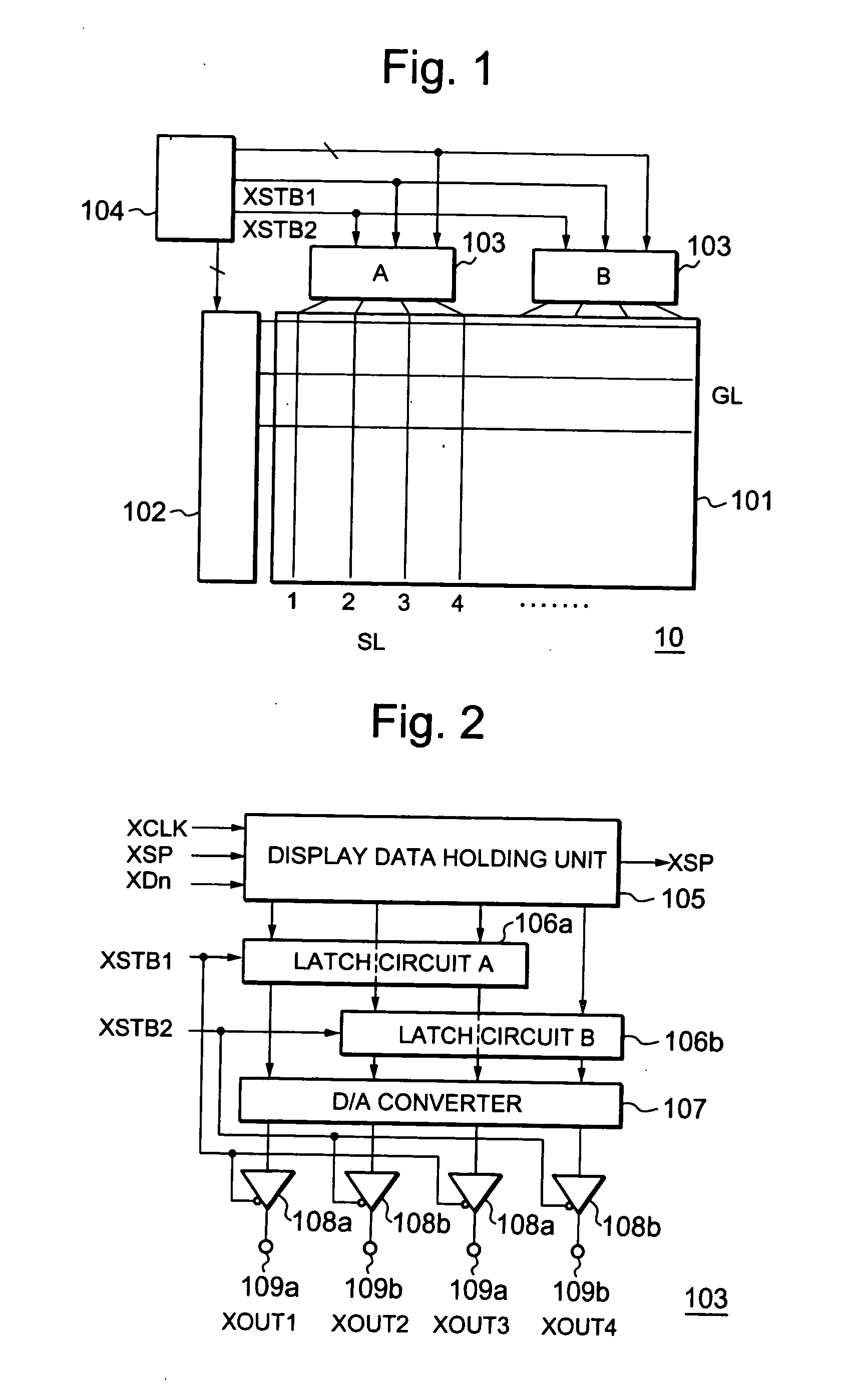
[0029] Descriptions will be provided for a display device according to a first embodiment of the present invention with reference to FIG. 1. Here, an active matrix liquid crystal display device of transmissive type will be described as an example of the display device. FIG. 1 is a schematic diagram of a liquid crystal display device 100 according to this embodiment. The liquid crystal display device 100 includes a liquid crystal display panel 101 for displaying images; a scan line driver (hereinafter referred to as a “gate driver”) 102 for driving scan lines (hereinafter referred to as “gate lines GL”); data line drivers 103 each for driving data lines (hereinafter referred to as “source lines SL”). This figure shows an example where two source drivers 103 are arranged. A source driver A 103a and a source driver B 103b are shown in FIG. 1. Each of the source drivers 103 is fabricated as a semiconductor chip. In addition, the liquid crystal display device 100 includes a controller 10...

second embodiment

[0057] The first embodiment has been described giving the example where display data are in the form of digital signals. However, display data may be in the form of analogue signals. In other words, display data in the form of analogue signals may be expanded and held in a sample hold circuit configured of a plurality of switches and a plurality of condensers.

[0058]FIG. 6 is a circuit diagram showing a source driver 103 according to the second embodiment. As shown in FIG. 6, the source driver 103 according to the second embodiment includes a display data holding unit 105, a first sample hold circuit A 112a, a second sample hold circuit B 112b, a D / A converter 107 and output buffers 111. What makes this embodiment different from the first embodiment is that the first latch circuit A 106a shown in FIG. 2 is replaced with the first sample hold circuit A 112a, and the second latch circuit B 106b shown in FIG. 2 is replaced with the second sample hold circuit B 112b.

[0059] The input of...

third embodiment

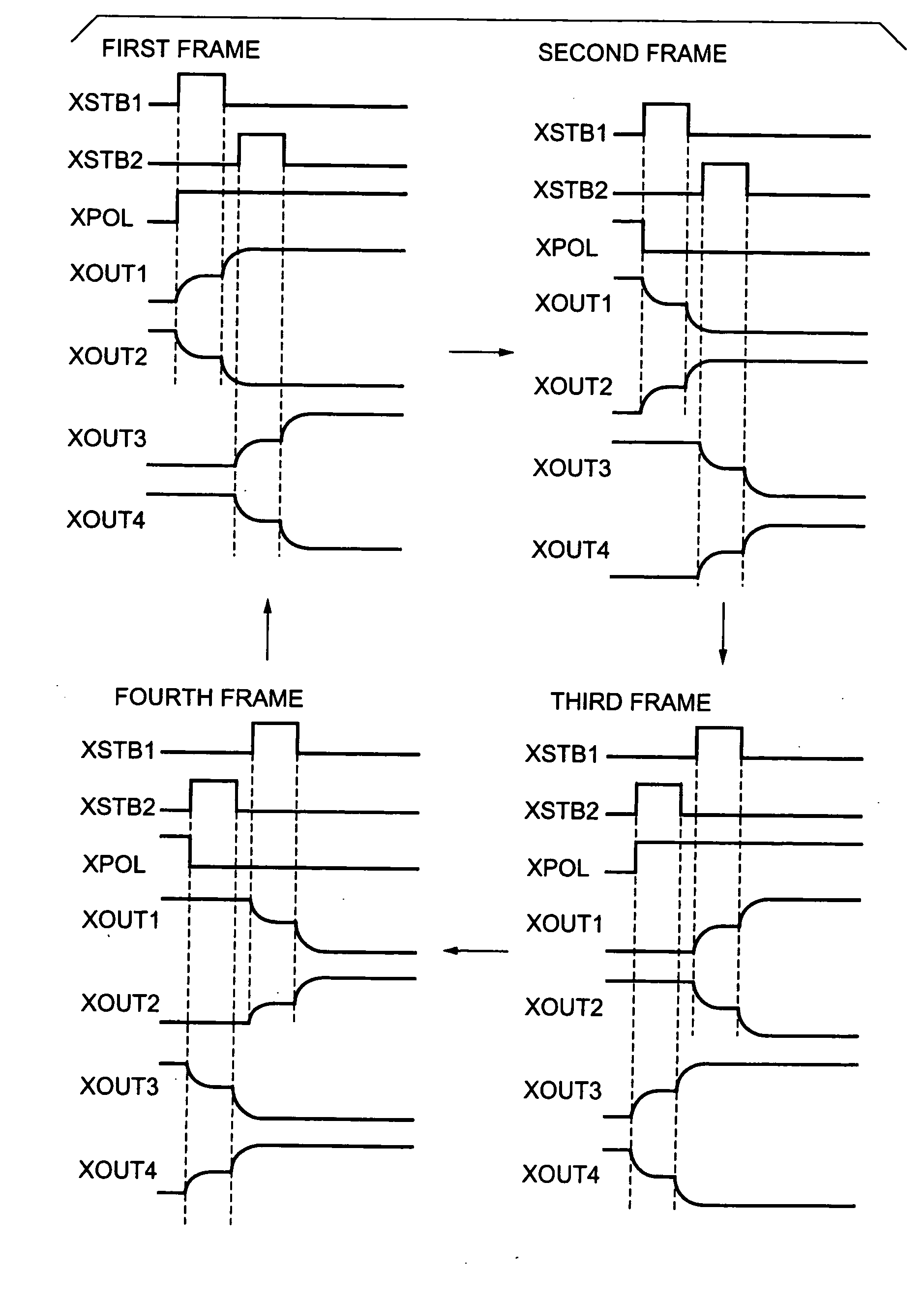
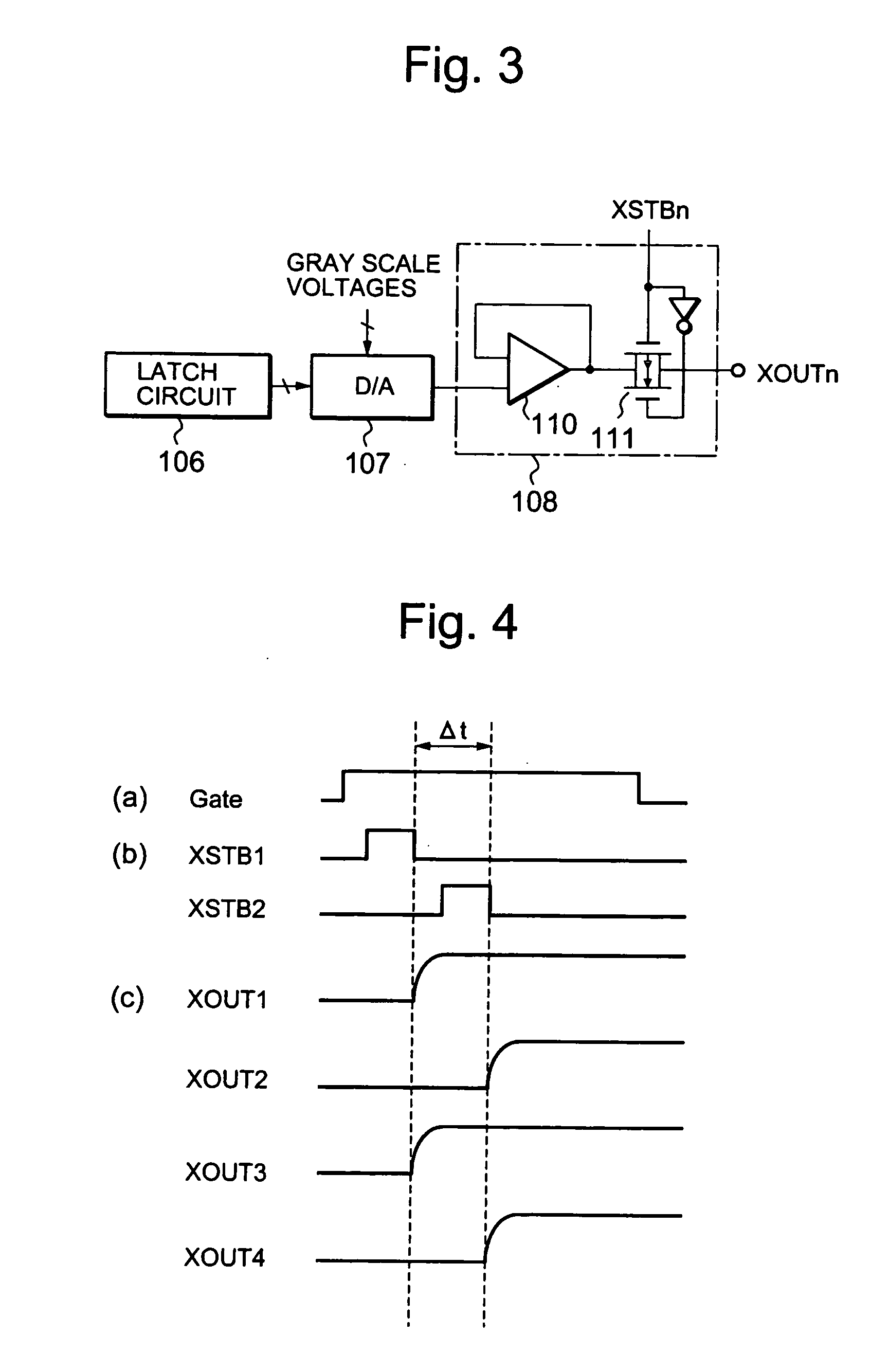
[0067] In the cases of the first embodiment and the second embodiment, the timing of the image-output control signal 1 (XSTB1) and the timing of the image-output control signal 2 (XSTB2) are different from each other by Δt. Time spent to write the image signal into the pixel electrodes connected to the odd-numbered source lines is longer by Δt than into the pixel electrodes connected to the even-numbered source lines. If it could take a sufficient time to write the image signal into the pixel electrodes, there would be no influence on the image quality. If the display panel is made larger and more precise, not only the load capacity becomes larger, but also one horizontal period becomes shorter.

[0068] For this reason, with regard to the odd-numbered source lines and the even-numbered source lines in the liquid crystal display panel 101, columns of pixel electrodes into which the image signal is insufficiently written alternate with columns of pixel electrodes into which the image s...


PUM


Abstract

A source driver according to an aspect of the present invention is a source driver for outputting image signals to an image-signal output terminal, and outputs image signals to an image-signal output terminal with a plurality of timings including a first timing and a second timing, which is different from the first timing, in response to a plurality of image-output control signals including a first and a second image-output control signals which are supplied from the outside during the same horizontal period.

Description

BACKGROUND OF THE INVENTION [0001] 1. Field of the Invention [0002] The present invention relates to a drive circuit chip for a display device and a display device in which the drive circuit chip is used. Particularly, the present invention relates to control of timings of the drive circuit chip. [0003] 2. Description of Related Art [0004] In these years, high development of the video / information-oriented society and increasingly wider use of multi-media systems have more and more increased the importance of flat displays such as liquid crystal display devices. Liquid crystal display devices have advantages including low power consumption, thinness and light weight. This has made liquid crystal devices widely used for display devices such as mobile terminal devices. [0005] Passive matrix liquid crystal display devices and active matrix liquid crystal display devices have been heretofore known as liquid crystal display devices (see Japanese Patent Laid-open applications No. Hei. 01-2...

Claims


Application Information

Patent Timeline
Patent Type & Authority Applications(United States)
IPC IPC(8): G06F3/12
CPCG09G3/3614G09G3/3677G09G3/3688G09G2310/027G09G2330/025G09G2330/06
Inventor SATOU, KOUICHIHASHIMOTO, YOSHIHARU
Owner NEC ELECTRONICS CORP
Why Eureka
Try Eureka