Eureka AIR delivers breakthrough ideas for toughest innovation challenges, trusted by R&D personnel around the world.

Semiconductor wafer positioning method, and apparatus using the same

Inactive Publication Date: 2006-08-31
NITTO DENKO CORP
View PDF2 Cites 10 Cited by
  • Summary
  • Abstract
  • Description
  • Claims
  • Application Information

AI Technical Summary

Benefits of technology

[0010] The present invention has been made in view of aforementioned circumstances. It is therefore a main object of the present invention to provide a semiconductor wafer positioning method capable of obtaining, with high accuracy, the position of a detection site formed in a peripheral edge of a semiconductor wafer with an inexpensive configuration, and to provide an apparatus using the method.

Problems solved by technology

However, the conventional method involves the following problem.
Therefore, the photoreception sensor cannot be received the projected light in the V notch portion
However, there is a problem that it is difficult to incorporate an image processing system in a conventional apparatus.
Further, since an image processing system is expensive, there is caused a disadvantage that a burden of the installment cost is large.

Method used


Image

  • Semiconductor wafer positioning method, and apparatus using the same
  • Semiconductor wafer positioning method, and apparatus using the same
  • Semiconductor wafer positioning method, and apparatus using the same

Examples


Embodiment Construction

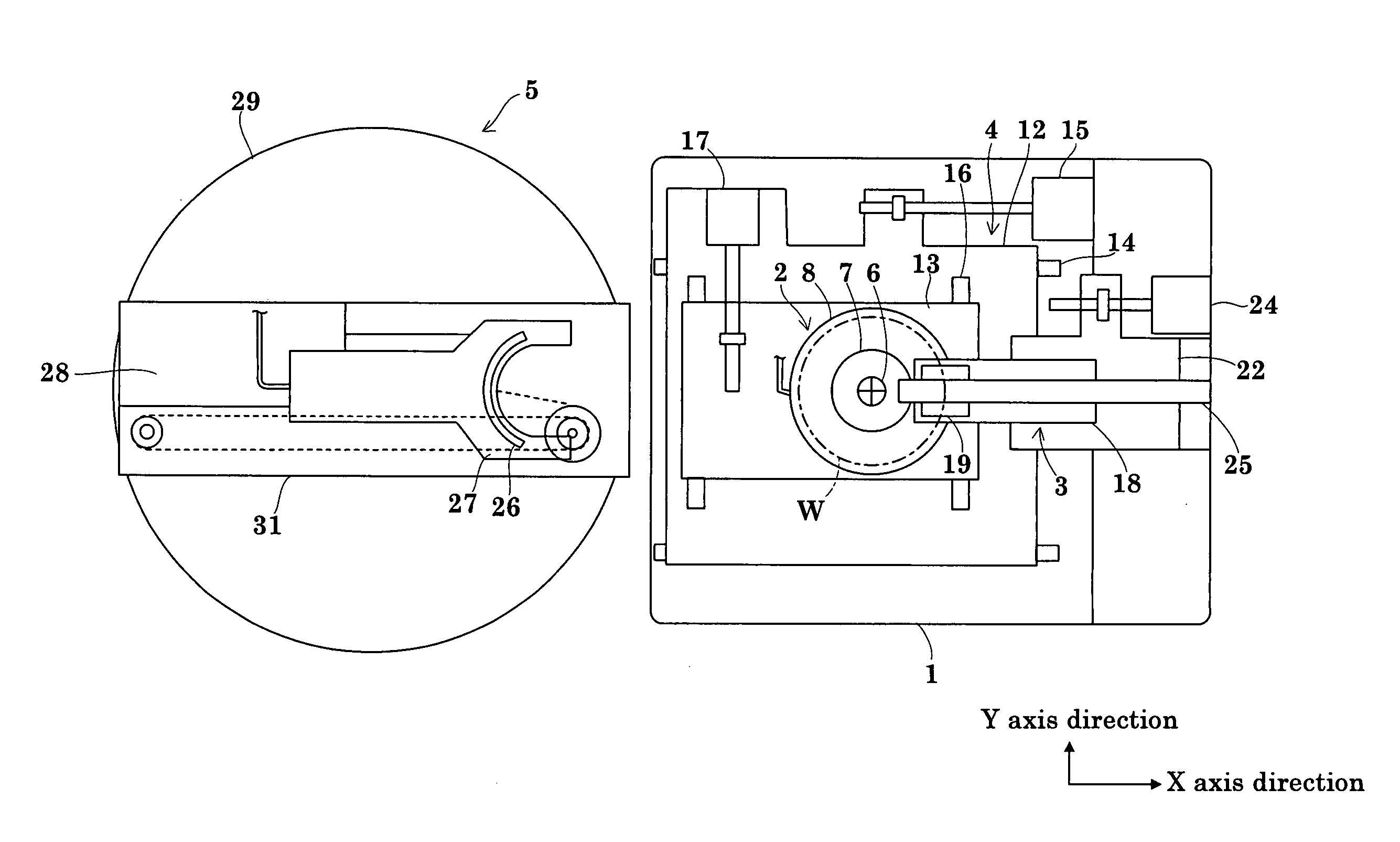
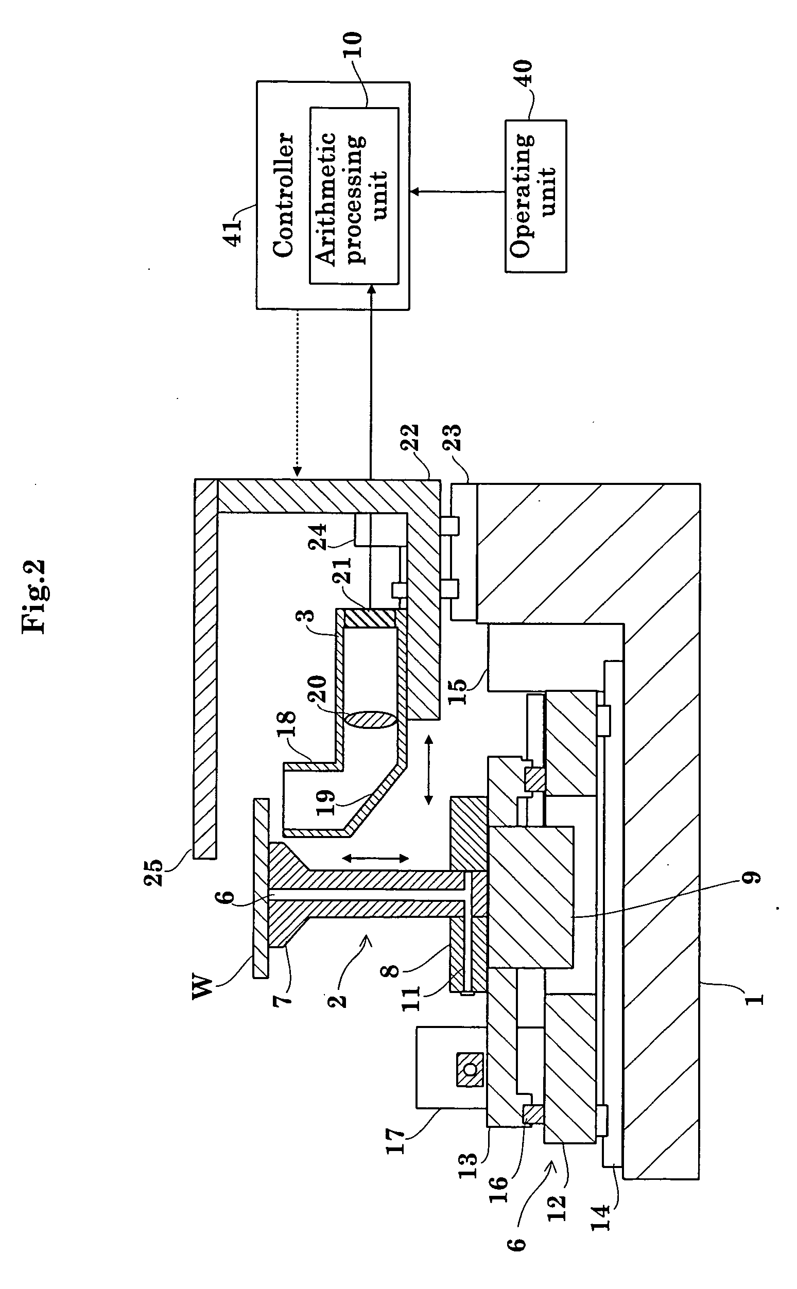
[0042] Hereinafter, an embodiment of a semiconductor wafer positioning apparatus according to the present invention will be explained with reference to the drawings.

[0043]FIG. 1 is a plan view showing a semiconductor wafer positioning apparatus according to an embodiment of the present invention, and FIG. 2 is a front view showing the main part of the configuration of the semiconductor wafer positioning apparatus.

[0044] As shown in FIG. 1, an apparatus for determining the center of a semiconductor wafer of the present invention includes: a rotating mechanism 2 for holding and rotating a semiconductor wafer (hereinafter, simply referred to as a “wafer”) W; a peripheral edge measuring mechanism 3 for measuring the peripheral edge of the wafer W held by the rotating mechanism 2; an arithmetic processing unit (not shown) for collecting an rotational angle of the rotating mechanism 2 and positional data of the peripheral edge of the wafer W relative to the rotational angle, and perform...


PUM


Abstract

The intensity of light of a predetermined wavelength corresponding to the type of a protective tape joined to the surface of a semiconductor wafer is adjusted by a controller, and a holding stage for holding the semiconductor wafer is scanned rotationally. At this time, at a V notch portion for positioning formed in the semiconductor wafer, light is transmitted through the protective sheet covering the surface, which is received by a photoreception sensor. Based on the change in the reception amount of light in the photoreception sensor, the position of a detection site is specified.

Description

BACKGROUND OF THE INVENTION [0001] (1) Field of the Invention [0002] The present invention relates to a semiconductor wafer positioning method for determining a handling position of a semiconductor wafer having a detection site such as a V notch or an orientation flat at a peripheral edge thereof based on positional information of the detection site, and relates to an apparatus using the method. [0003] (2) Description of the Related Art [0004] A semiconductor wafer (hereinafter, simply referred to as a “wafer”) is subjected to back surface processing performed by a mechanical method such as grinding or polishing, a chemical method using etching, or the like, so that the thickness thereof is reduced. When the wafer is processed by using such a method, a protective tape is joined to the wafer surface so as to protect the surface on which a wiring pattern has been formed. For the polished wafer on which the protective tape is joined, positional information of the peripheral edge is obt...

Claims


Application Information

Patent Timeline
IPC IPC(8): H01L21/76H01L21/02H01L21/68
CPCH01L21/681Y10S414/136H01L21/68
Inventor IKEDA, SATOSHIYAMAMOTO, MASAYUKI
Owner NITTO DENKO CORP
Why Eureka
Eureka Blog
Learn More