Semiconductor device

Active Publication Date: 2006-09-07
KK TOSHIBA
View PDF5 Cites 83 Cited by
  • Summary
  • Abstract
  • Description
  • Claims
  • Application Information

AI Technical Summary

Benefits of technology

[0010] In one aspect the present invention provides a semiconductor device, comprising: a semiconductor substrate; a plurality of first semiconductor regions of a first conduction type formed by disposing a single crystal semiconductor layer of the first conduction type on a surface of the semiconductor substrate and providing a plurality of trenches in the single crystal semiconductor layer, the plurality of first semiconductor regions being formed at intervals in a direction parallel to the surface; and a plurality of second semiconductor regions of a second conduction type formed of an epitaxial layer buried in the plurality of trenches, the plurality of second semiconductor regions each including an outer portion with a high impurity concentration formed against an inner wall of the trench, and an inner portion with a low impurity concentration formed inner than the outer portion.
[0011] In another aspect the present invention provides a semiconductor device, comprising a semiconductor substrate; a plurality of first semiconductor regions of a first conduction type formed by disposing a single crystal semiconductor layer of the first conduction type on a surface of the semiconductor substrate and providing a plurality of trenches in the single crystal semiconductor layer, the trenches each hav

Problems solved by technology

Therefore, lowering the on-resistance may require an increase in the impurity concentration in the drift region to lower the electrical resistance of the drift r

Method used


Image

  • Semiconductor device
  • Semiconductor device
  • Semiconductor device

Examples


first embodiment

(Major Effect of First Embodiment)

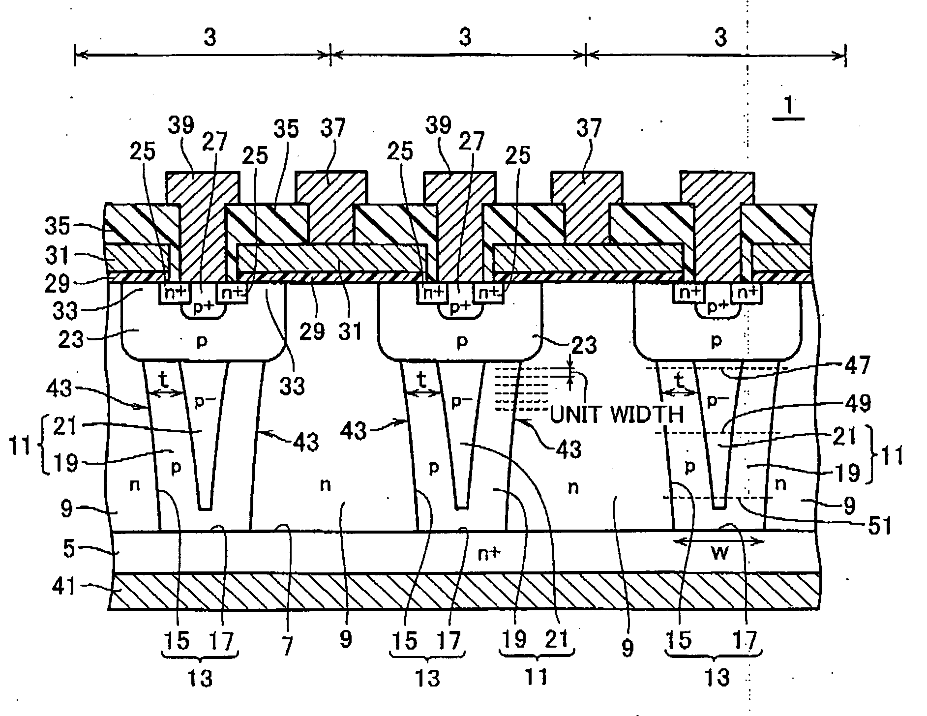
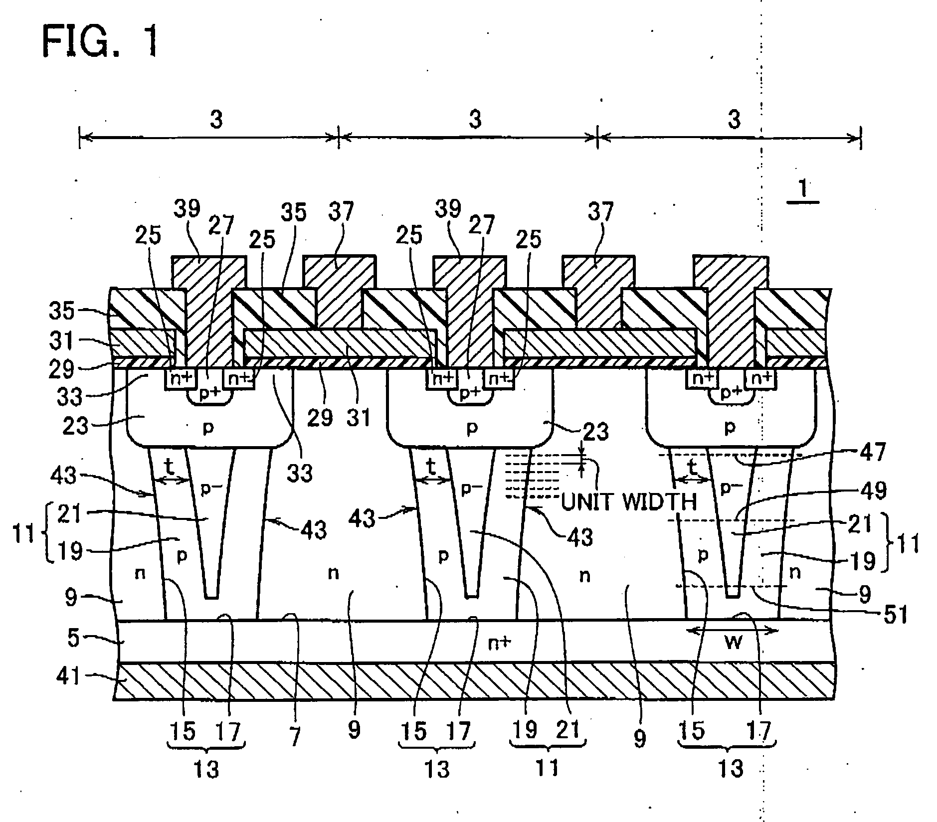
[0055] The semiconductor device 1 shown in FIG. 1 according to the first embodiment is possible to improve the charge balance between the first and second semiconductor regions 9, 11 and enhance the breakdown voltage. This effect is described in comparison with a comparative example. FIG. 2 is a vertical cross-sectional view of part of a semiconductor device 45 according to the comparative example, which corresponds to FIG. 1. The semiconductor device 45 comprises p-type second semiconductor regions 11, which are not divided into the outer portion and the inner portion and have an overall impurity concentration of “p”. This is different from the first embodiment.

[0056] Hereinbelow, in order to clarify the effect of the embodiment, explanation are performed, wherein the first and second semiconductor regions 9 and 11 in FIG. 1 and FIG. 2 are divided by a unit width (i.e. 1 micrometer; see FIG. 1) respectively, in a direction from the surface 7 towar...

second embodiment

[0074]FIG. 10 is a vertical cross-sectional view of part of a semiconductor device 63 according a second embodiment. In the second embodiment, the first semiconductor region 9 is also composed of an outer portion 65 and an inner portion 67. The outer portion 65 and the inner portion 67 both are of n-type. The impurity concentration is higher in the outer portion 65 than in the inner portion 67 the outer portion 65 has an impurity concentration of “n” while the inner portion 67 has an impurity concentration of “n−”.

[0075] The outer portion 65 in the first semiconductor region 9 is formed opposite the outer portion 19 of the second semiconductor region 11 and against the side 15 of the trench 13. The outer portion 65 has an upper end brought into contact with the base region 23 and a lower end brought into contact with the semiconductor substrate 5. On formation of the outer portion 65, the thickness thereof is almost constant. The limitation, “on formation of the outer portion 65”, ...

third embodiment

[0082]FIG. 13 is a vertical cross-sectional view of part of a semiconductor device 71 according a third embodiment. The regions N1, N2, . . . Nm has impurity concentrations controlled to elevate as becoming more distant from the surface 7 of the semiconductor substrate. This is a difference between the third embodiment and the first embodiment shown in FIG. 1. FIG. 13 shows the elevation of the n-type impurity concentration as “n−−, n−, n”. The impurity concentration may be controlled to elevate in the form of steps or in the form of a smooth curve or straight line.

[0083] Both in the first and third embodiments, the inner portion 21 with the impurity concentration of “p−” has the width that extends as becoming more distant from the surface 7. Therefore, the number of impurity atoms in the inner portion 21 of the regions P1, P2, . . . Pm increases more or less as becoming more distant from the surface 7. The impurity concentration in the inner portion 21 is relatively small and negl...


PUM


Abstract

A single crystal semiconductor layer of a first conduction type is disposed on a surface of a semiconductor substrate. A plurality of trenches are provided in the semiconductor layer to form a plurality of first semiconductor regions of the first conduction type at intervals in a direction parallel to the surface. An epitaxial layer is buried in the plurality of trenches to form a plurality of second semiconductor regions of a second conduction type. The plurality of second semiconductor regions each includes an outer portion with a high impurity concentration formed against an inner wall of the trench, and an inner portion with a low impurity concentration formed inner than the outer portion.

Description

CROSS REFERENCE TO RELATED APPLICATION [0001] This application is based on and claims the benefit of priority from prior Japanese Patent Application No. 2005-55369, filed on Mar. 1, 2005, the entire contents of which are incorporated herein by reference. BACKGROUND OF THE INVENTION [0002] 1. Field of the Invention [0003] The present invention relates to a semiconductor device such as a power MOSFET (Metal Oxide Semiconductor Field Effect Transistor). [0004] 2. Description of the Related Art [0005] A power semiconductor device, typically a power MOSFET, comprises a semiconductor chip structured such that a plurality of cells having commonly connected gates are formed in an epitaxial layer (semiconductor region) disposed on a semiconductor substrate. The power MOSFET, having a low on-resistance and a possibility of fast switching, can control a high-frequency large current efficiently. Accordingly, the power MOSFET has been used widely as a small power converter such as a component of...

Claims


Application Information

Patent Timeline
IPC IPC(8): H01L29/76H01L21/336
CPCH01L29/0634H01L29/1095H01L29/66712H01L29/7802
Inventor TOKANO, KENICHIMATSUDA, TETSUOSAITO, WATARU
Owner KK TOSHIBA
Why Eureka
Try Eureka