Semiconductor device including a semiconductor chip with signal contact areas and supply contact areas, and method for producing the semiconductor device

a semiconductor chip and semiconductor technology, applied in semiconductor devices, semiconductor/solid-state device details, electrical devices, etc., can solve the problem of limited connection elements now exclusively, and achieve the effect of increasing power consumption and more spa

Inactive Publication Date: 2006-09-07
INFINEON TECH AG
View PDF11 Cites 21 Cited by
  • Summary
  • Abstract
  • Description
  • Claims
  • Application Information

AI Technical Summary

Benefits of technology

[0010] The present invention solves the problem, for large scale integrated semiconductor devices, of the increasing power consumption and to overcome the abovementioned disadvantages in the prior art. The present invention reduces the number of supply connections externally toward a substrate or toward a flat conductor leadframe, so that more space is created for signal connections.

Problems solved by technology

Rather, the connecting elements are now limited exclusively to the active top side of the semiconductor chip.

Method used


Image

  • Semiconductor device including a semiconductor chip with signal contact areas and supply contact areas, and method for producing the semiconductor device
  • Semiconductor device including a semiconductor chip with signal contact areas and supply contact areas, and method for producing the semiconductor device
  • Semiconductor device including a semiconductor chip with signal contact areas and supply contact areas, and method for producing the semiconductor device

Examples


first embodiment

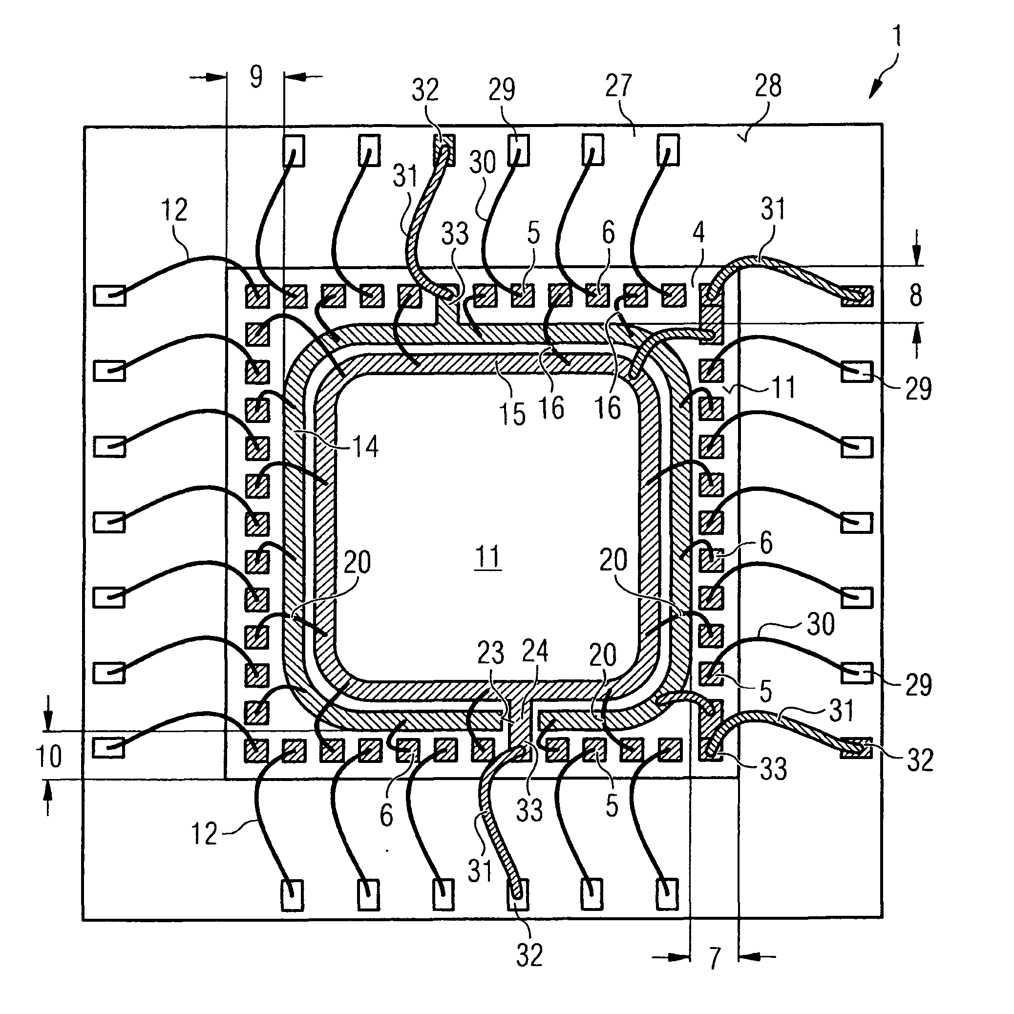
[0040]FIG. 1 schematically shows a plan view of a semiconductor device 1 of the invention. This semiconductor device 1 includes a wiring substrate 27 with a top side 28, the areal extent of which is greater than the areal extent of a semiconductor chip 4. FIG. 1 depicts the active top side 11 of the semiconductor chip 4, in which case a plastic housing composition in which the semiconductor chip 4 and the wiring substrate 27 are embodied has been omitted in order to better illustrate the invention.

[0041] Signal contact areas 5 and supply contact areas 6 are arranged alternately in the edge regions 7, 8, 9 and 10 of the top side 11 of the semiconductor chip 4. In conventional semiconductor devices, signal contact areas 5 and supply contact areas 6 arranged in the edge regions 7, 8, 9 and 10 are electrically connected to corresponding contact pads 29 on the top side 28 of the wiring substrate 27 by connecting elements 12.

[0042] In this embodiment of the invention, connecting elements...

second embodiment

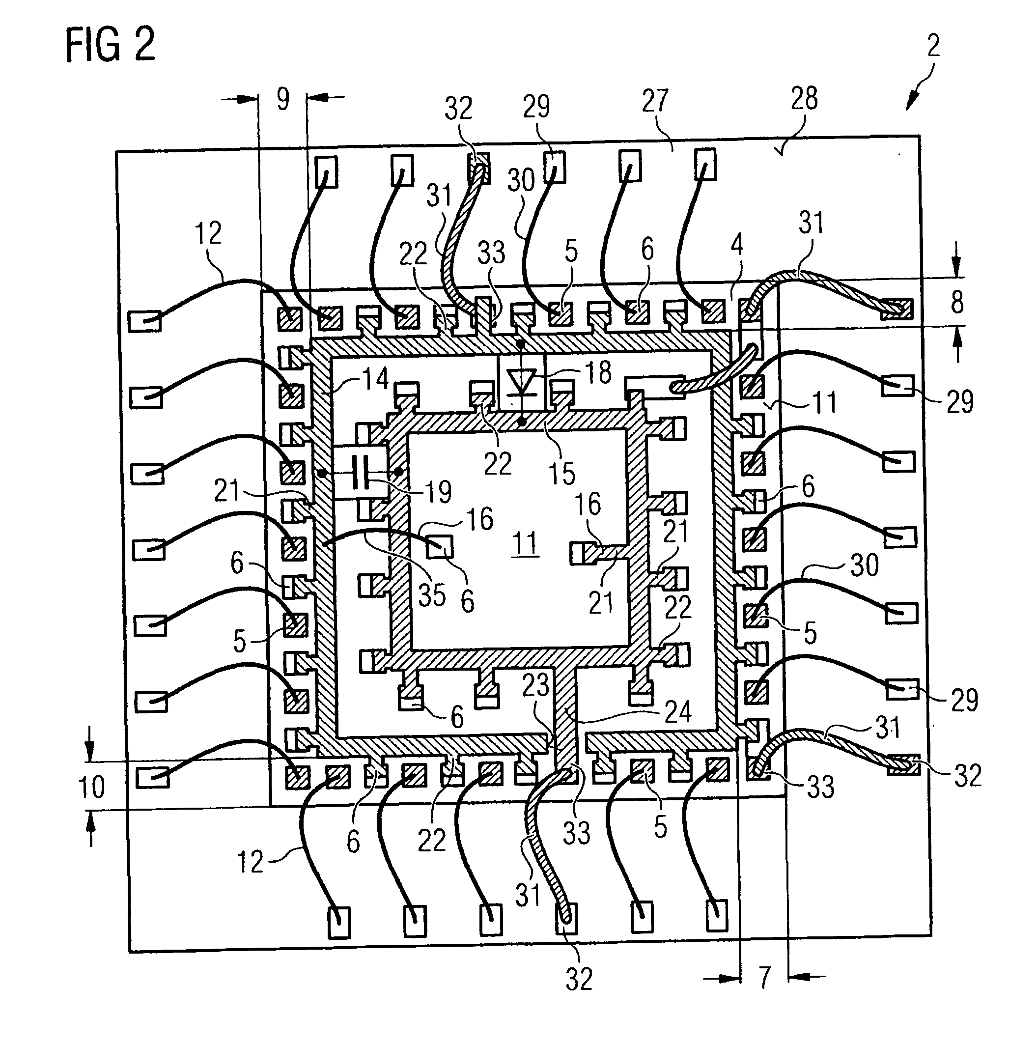
[0047]FIG. 2 shows a schematic plan view of a semiconductor device 2 of the invention. Components having functions identical to those of FIG. 1 are identified by the same reference symbols and are thus not described again.

[0048] In this second embodiment of the invention, only the connecting elements 12 to contact pads 29 on the top side 28 of the wiring substrate 27 are produced from bonding wires 30, while the internal connections are formed with bonding lugs 22. Bonding wires 35 are used as internal connecting elements 16 only in the cases in which the supply collective electrodes 14 or 15 are to be bridged on the top side 11 of the semiconductor chip 4. Instead of bonding lugs 22, the connections between supply contact areas 6 and the supply collective electrodes 14 or 15 are also produced by conductor tracks 21.

[0049] The difference between bonding lugs 22 and conductor tracks 21 is that bonding lugs can be produced together with the patterning of metal foils for the supply co...

third embodiment

[0052]FIG. 4 shows a schematic cross-section through a semiconductor device 3 of the invention. Components having functions identical to those in FIG. 1 are identified by the same reference symbols and are thus not further described.

[0053] In this third embodiment of the invention, the two supply collective electrodes 14 and 15 are arranged in a stack one above another and are electrically insulated from one another by an insulation layer 17. The areal extent of the lower supply collective electrode 14 is greater than the areal extent of the upper supply collective electrode 15, with the result that internal connecting elements 16 can be led both to the lower supply collective electrode 14 and to the upper supply collective electrode 15 without short circuits arising. Moreover, connecting elements 12 can thus be led to the wiring substrate 27, which connecting elements have thicker bonding wires 31 than the internal connecting elements 16 with their bonding wires 20. While the suppl...


PUM


Abstract

A semiconductor device includes a semiconductor chip, where the semiconductor chip includes signal contact areas and supply contact areas. The signal contact areas are arranged on edge regions of the active top side of the semiconductor chip and are electrically connected to external signal exterior connections of the semiconductor device by connecting elements. The active top side of the semiconductor chip includes at least two supply collective electrodes made of annularly patterned metal foils which are arranged within the signal contact areas and are affixed in an electrically insulating manner on the top side. The supply collective electrodes are electrically connected to the supply contact areas of the semiconductor chip by internal connecting elements.

Description

CROSS REFERENCE TO RELATED APPLICATIONS [0001] This application claims priority under 35 USC §119 to German Application No. DE 10 2005 009 163.6, filed on Feb. 25, 2005, and titled “Semiconductor Device Having a Semiconductor Chip, Which Has Signal Contact Areas and Supply Contact Areas, and Method for Producing the Semiconductor Device,” the entire contents of which are hereby incorporated by reference. FIELD OF THE INVENTION [0002] The invention relates to a semiconductor device including a semiconductor chip, which has signal contact areas and supply contact areas, and to a method for producing the semiconductor device. BACKGROUND [0003] The number of signal contact areas and supply contact areas is constantly increasing for large scale integrated semiconductor devices, while the area requirement per switching function is constantly decreasing. This is realized by advanced miniaturization of the circuit structures on a semiconductor chip with each new technology generation, which...

Claims


Application Information

Patent Timeline
Patent Type & Authority Applications(United States)
IPC IPC(8): H01L23/52
CPCH01L23/50H01L23/5286H01L24/05H01L24/06H01L24/45H01L24/48H01L24/49H01L2224/0401H01L2224/04042H01L2224/05552H01L2224/05556H01L2224/05639H01L2224/05644H01L2224/45015H01L2224/45124H01L2224/45144H01L2224/48091H01L2224/4813H01L2224/48227H01L2224/48465H01L2224/48471H01L2224/4903H01L2224/49051H01L2224/4911H01L2924/01005H01L2924/01013H01L2924/01015H01L2924/01029H01L2924/01047H01L2924/01074H01L2924/01079H01L2924/01082H01L2924/014H01L2924/09701H01L2924/12044H01L2924/13091H01L2924/14H01L2924/15311H01L2924/19041H01L2924/20755H01L2924/20756H01L2924/20757H01L2924/20758H01L2924/20759H01L2924/2076H01L2924/30107H01L2924/01023H01L2924/01033H01L2224/48233H01L2224/73265H01L2224/48644H01L2224/48639H01L2224/48739H01L2224/73215H01L2224/05551H01L2924/12041H01L2224/05554H01L2224/0603H01L2924/00014H01L2924/00H01L2224/48744H01L2924/15787H01L2924/181H01L2224/32225H01L2224/023H01L2924/00012H01L2924/0001
Inventor PAPE, HEINZ
Owner INFINEON TECH AG
Why Eureka
Try Eureka