Method and apparatus for identifying and correcting phase conflicts

a phase conflict and mask technology, applied in the field of semiconductor chip design and fabrication, can solve the problems of difficult printing of features that are smaller than needing phase shifters, and difficult capture of constraints with traditional design rules, and achieve the problem of not being able to solve the phase assignment problem on the corresponding psm-layout, and unable to solve the problem of a certain threshold width

Active Publication Date: 2006-09-07
SYNOPSYS INC
View PDF4 Cites 4 Cited by
  • Summary
  • Abstract
  • Description
  • Claims
  • Application Information

AI Technical Summary

Benefits of technology

[0011] One embodiment of the present invention provides a system that identifies a set of phase conflicts in a layout that when corrected will render the layout phase-assignable. During operation, the system constructs a phase-conflict graph from a PSM-layout such that the PSM-layout is phase-assignable if and only if the phase-conflict graph is bipartite. (Note that the instant application describes systems and techniques in the context of a PSM-layout. But, it will be apparent that these systems and techniques can easily be applied to a PSM-mask.) The system then removes a first set of edges from the phase-conflict graph to create a planar sub-graph. Next, the system removes a second set of edges from the planar sub-g

Problems solved by technology

Typically, features that are smaller than a certain threshold width are difficult to print and need to have phase shifters around them.
It is hard to capture these constraints with traditional design rules used in layout generation like minimum width and spacing rules.
Hence, it is highly likely that there will be a layout that satisfies all the design rules, and yet it is impossible to solve the phase assignment problem on its corresponding PSM-layout due

Method used


Image

  • Method and apparatus for identifying and correcting phase conflicts
  • Method and apparatus for identifying and correcting phase conflicts
  • Method and apparatus for identifying and correcting phase conflicts

Examples


Embodiment Construction

Integrated Circuit Design and Fabrication

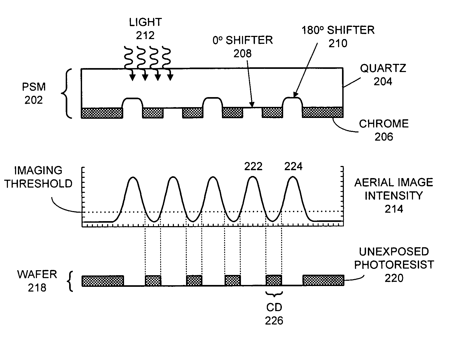
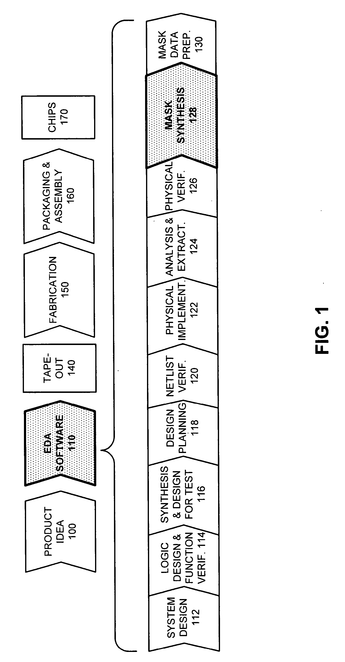
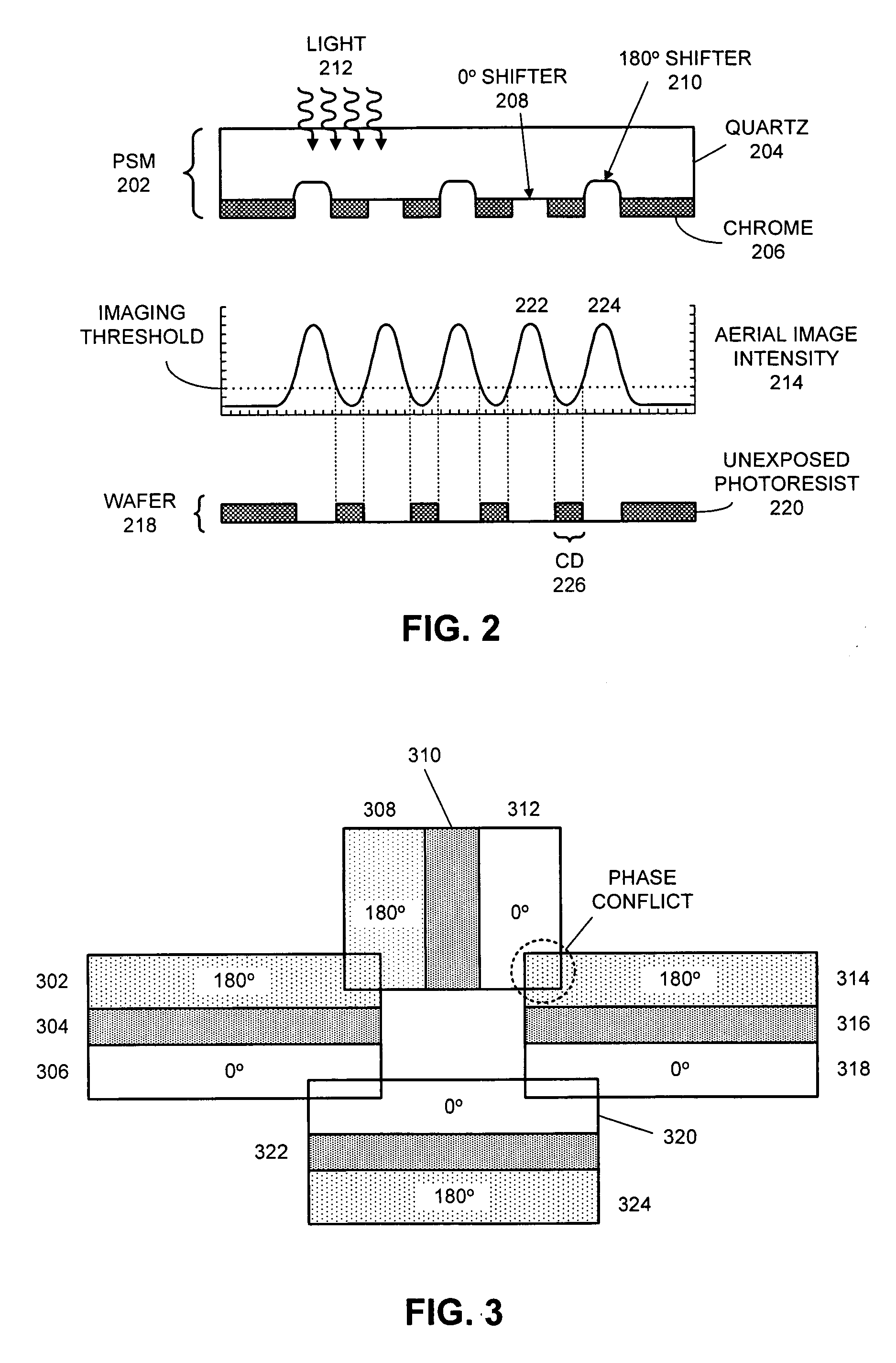
[0030]FIG. 1 illustrates various steps in the design and fabrication of an integrated circuit in accordance with an embodiment of the present invention. The process starts with a product idea (step 100). Next, the product idea is realized using an integrated circuit, which is designed using Electronic Design Automation (EDA) software (step 110). Once the circuit design is finalized, it is taped-out (step 140). After tape-out, the process goes through fabrication (step 150), packaging, and assembly (step 160). The process eventually culminates with the production of chips (step 170).

[0031] The EDA software design step 110, in turn, includes a number of sub-steps, namely, system design (step 112), logic design and function verification (step 114), synthesis and design for test (step 116), design planning (step 118), netlist verification (step 120), physical implementation (step 122), analysis and extraction (step 124), physical verification (s...


PUM


Abstract

One embodiment of the present invention provides a system that identifies a substantially minimal set of phase conflicts in a PSM-layout that when corrected renders the layout phase-assignable. During operation, the system constructs a phase-conflict graph from a PSM-layout such that the PSM-layout is phase-assignable if and only if the phase-conflict graph is bipartite. Next, the system removes a first set of edges from the phase-conflict graph to make the graph planar, and then removes a second set of edges to make the graph bipartite. The system then adds zero or more edges of the first set of edges, and determines a set of phase conflicts in the PSM-layout based on the remaining edges in the first set of edges and the second set of edges. The system can also be used to correct a given set of phase conflicts in a PSM-layout. The system identifies a set of lines in the layout, such that adding space along the set of lines will result in a phase-assignable PSM-layout. A substantially minimal set of lines can be determined by solving an equivalent minimum-weight set covering problem.

Description

RELATED APPLICATIONS [0001] This application hereby claims priority under 35 U.S.C. §119 to U.S. Provisional Patent Application No. 60 / 659,581, filed on 7 Mar. 2005, entitled “Method and apparatus for identifying and correcting phase conflicts,” by inventors Subarnarekha Sinha and Charles C. Chiang (Attorney Docket No. SNPS-P0650P).BACKGROUND [0002] 1. Field of the Invention [0003] The present invention relates to the process of designing and fabricating semiconductor chips. More specifically, the present invention relates to a method and an apparatus for identifying and correcting phase conflicts in a phase shift mask or layout. [0004] 2. Related Art [0005] The relentless miniaturization of integrated circuits has been a key driving force behind technological innovation. This miniaturization has been made possible by significant improvements in various fabrication technologies. [0006] Phase shift mask (PSM) technology is one such improvement. In PSM technology, phase shifters are i...

Claims


Application Information

Patent Timeline
IPC IPC(8): G03C5/00G03F9/00G06F17/50G03F1/00
CPCG03F1/30
Inventor SINHA, SUBARNAREKHACHIANG, CHARLES C.
Owner SYNOPSYS INC
Why Eureka
Try Eureka