Single or multi-color high efficiency light emitting diode (LED) by growth over a patterned substrate

a light-emitting diode, single or multi-color technology, applied in the direction of electrical equipment, semiconductor devices, radio frequency control devices, etc., can solve the problems of low yield, limited index contrast of materials epitaxially grown, and loss of most of the light emitted within the semiconductor led material, etc., to achieve high extraction efficiency

Inactive Publication Date: 2006-09-14
RGT UNIV OF CALIFORNIA
View PDF20 Cites 73 Cited by
  • Summary
  • Abstract
  • Description
  • Claims
  • Application Information

AI Technical Summary

Benefits of technology

[0028] The present invention discloses a single or multi-color light emitting diode (LED) with high extraction efficiency comprised of a substrate, a buffer layer grown on the substrate, a patterned layer deposited on top of the buffer layer and an active layer formed on the patterned layer, for example by Lateral Epitaxial Overgrowth (LEO), and including one or more light emitting species. The patterned layer comprises a patterned, perforated or pierced mask (made of insulating, semiconducting or metallic material) and materials filling holes in the mask. The patterned layer, due to a large index difference with the active layer and / or variations of the refractive index between the mask and materials filling holes in the mask, both acts as an optical confinement layer and as a buried diffraction grating, thus controlling emissions of the active layer into radiative and guided modes, which are then extracted.

Problems solved by technology

Unfortunately, most of the light emitted within a semiconductor LED material is lost due to total internal reflection at the semiconductor-air interface.
This higher extraction efficiency is, however, limited to values in the 40% range as the micro-cavity structure also leads to very efficient emission into guided modes and leaky modes.
Difficulties are encountered in most materials systems when attempting to obtain large micro-cavity extraction improvements of LEDs. FIGS. 4B and 5B show the emission diagrams from which is extracted the expected efficiency of optimized GaN micro-cavity LEDs, and illustrate the following issues: (i) The index contrast for materials epitaxially grown is quite limited, in particular for the very important nitride materials.
It is difficult to obtain such thin active layers.
While lifting off the nitride materials (buffer layer and active layer) from the substrate is already a delicate operation, there is, in addition, extreme difficulty in obtaining the thinner layers (i.e., further removing part or all of the buffer layer) bounded by good metal mirrors, which would lead to the excellent performance of the thin metal mirror structure shown in FIG. 4A.

Method used


Image

  • Single or multi-color high efficiency light emitting diode (LED) by growth over a patterned substrate
  • Single or multi-color high efficiency light emitting diode (LED) by growth over a patterned substrate
  • Single or multi-color high efficiency light emitting diode (LED) by growth over a patterned substrate

Examples


Embodiment Construction

[0045] In the following description of the preferred embodiment, reference is made to the accompanying drawings which form a part hereof, and in which is shown by way of illustration a specific embodiment in which the invention may be practiced. It is to be understood that other embodiments may be utilized and structural changes may be made without departing from the scope of the present invention.

OVERVIEW

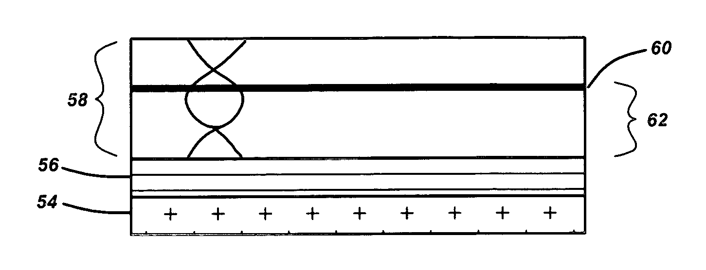
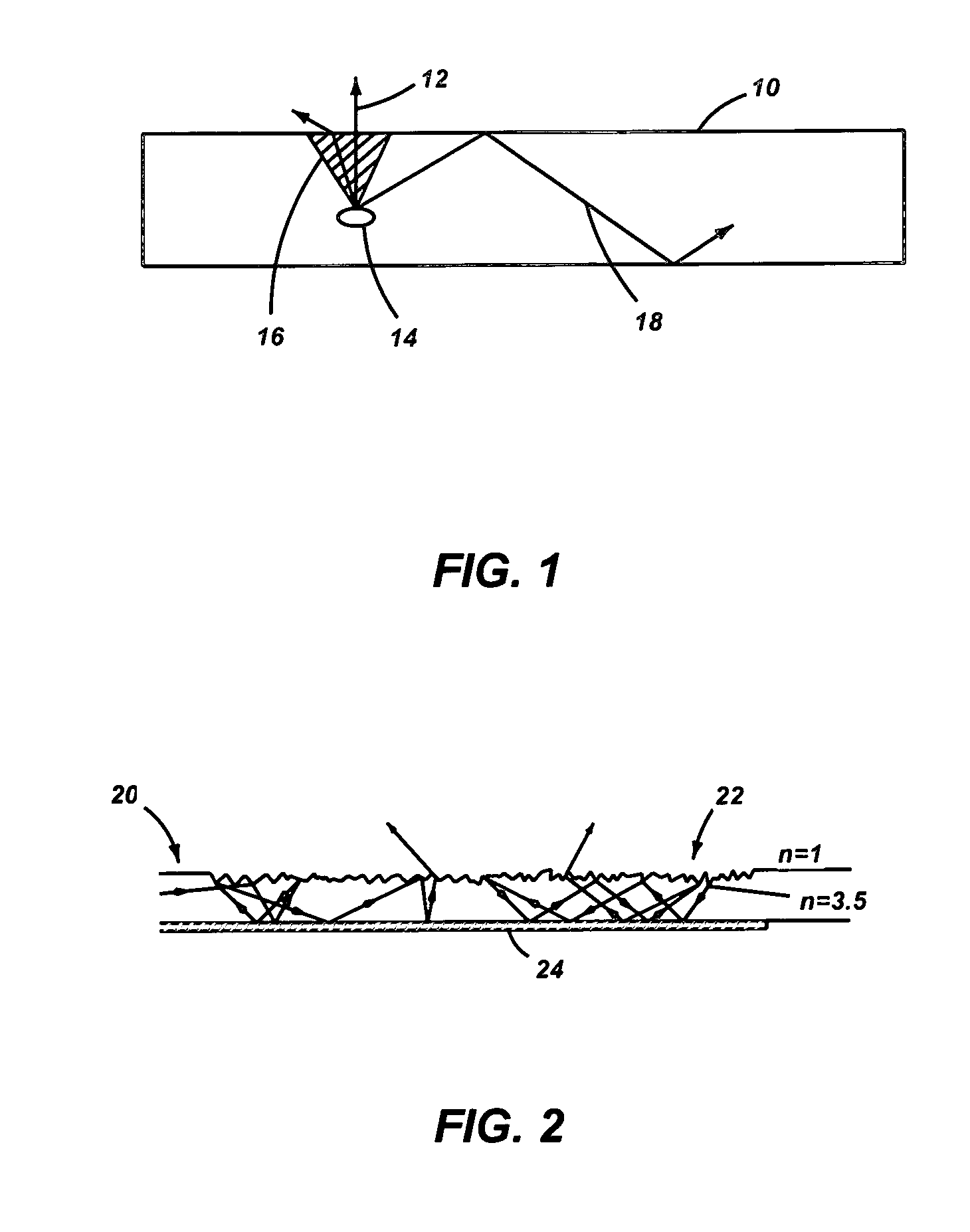
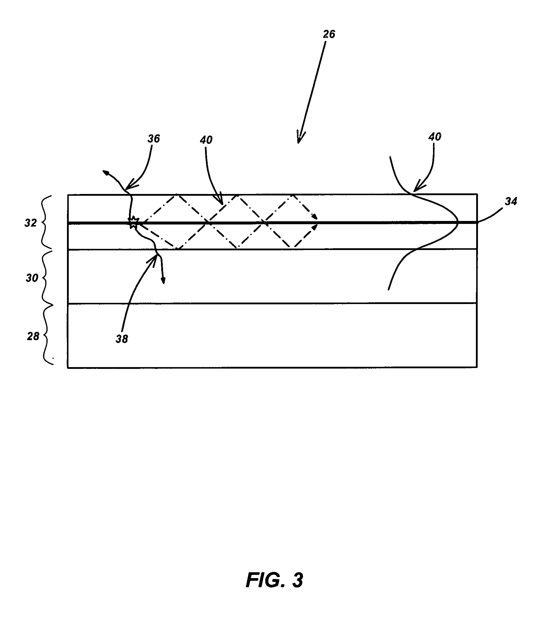
[0046] The present invention describes new LED structures that provide increased light extraction efficiency while retaining a planar structure. The planar structure makes the new LED structures easily manufacturable at low cost.

[0047] Preferably, the structure comprises a substrate, a buffer layer grown on the substrate, a patterned layer deposited on the buffer layer, and an active layer including one or more emitting species (some of which are current-injected) formed on the patterned layer, for example by Lateral Epitaxial Overgrowth (LEO). The patterned layer comprises a pa...


PUM


Abstract

A single or multi-color light emitting diode (LED) with high extraction efficiency is comprised of a substrate, a buffer layer formed on the substrate, one or more patterned layers deposited on top of the buffer layer, and one or more active layers formed on or between the patterned layers, for example by Lateral Epitaxial Overgrowth (LEO), and including one or more light emitting species, such as quantum wells. The patterned layers include a patterned, perforated or pierced mask made of insulating, semiconducting or metallic material, and materials filling holes in the mask. The patterned layer acts as an optical confining layer due to a contrast of a refractive index with the active layer and/or as a buried diffraction grating due to variation of a refractive index between the mask and the material filling the holes in the mask.

Description

CROSS-REFERENCE TO RELATED APPLICATIONS [0001] This application is related to the following co-pending and commonly-assigned applications: [0002] U.S. Utility application Ser. No. 10 / 938,704, filed Sep. 10, 2004, by Carole Schwach, Claude C. A. Weisbuch, Steven P. DenBaars, Henri Benisty, and Shuji Nakamura, entitled “WHITE, SINGLE OR MULTI-COLOR LIGHT EMITTING DIODES BY RECYCLING GUIDED MODES,” attorneys' docket number 30794.115-US-01 (2004-064-1), [0003] U.S. Utility application Ser. No. ______, filed on same date herewith, by Claude C. A. Weisbuch, Aurelien J. F. David, James S. Speck and Steven P. DenBaars, entitled “HORIZONTAL EMITTING, VERTICAL EMITTING, BEAM SHAPED, DISTRIBUTED FEEDBACK (DFB) LASERS BY GROWTH OVER A PATTERNED SUBSTRATE,” attorneys' docket number 30794.121-US-01 (2005-144-1), and U.S. Utility application Ser. No. ______, filed on same date herewith, by, Aurelien J. F. David, Claude C. A. Weisbuch and Steven P. DenBaars, entitled “HIGH EFFICIENCY LIGHT EMITTING...

Claims


Application Information

Patent Timeline
Patent Type & Authority Applications(United States)
IPC IPC(8): H01L33/00H01L33/20H01L33/22H01L33/24
CPCH01L33/20H01L33/22H01L33/24H01L2933/0083
Inventor WEISBUCH, CLAUDE C.A.DAVID, AURELIEN J.F.SPECK, JAMES S.DENBAARS, STEVEN P.
Owner RGT UNIV OF CALIFORNIA
Why Eureka
Try Eureka