Semiconductor memory and system apparatus

Inactive Publication Date: 2006-09-14
SOCIONEXT INC
View PDF3 Cites 12 Cited by
  • Summary
  • Abstract
  • Description
  • Claims
  • Application Information

AI Technical Summary

Benefits of technology

[0012] In a preferred embodiment of the first and second aspects of the present invention, a delay circuit delays the reset signal to generate a delayed reset signal. The mode register initializes the register part in response to the delayed reset signal in order to stop an output of the soft reset signal. For this reason, an output period of the soft reset signal can be easily set by a delayed time of the delay circuit, so that it is possible to reliably initialize the internal circuit. Moreover, as described above, since the mode register itself is initialized by the setting command, it is possible to control the system simply and easily.
[0013] In a preferred embodiment of the first and second aspects of the present invention, the register part of the mode register is set according to at least one of external address signals and external data signals supplied with the setting command. The soft reset signal is not output just by supplying an external command. Accordingly, it can be prevented that the setting command is recognized incorrectly due to noise or the like to thereby initialize the internal circuit incorrectly.
[0014] In a preferred embodiment of the first and second aspects of the present invention, a power-on reset part of the reset signal generator generates a power-on reset signal when an external power supply voltage is lower than a predetermined value. A synthesis part of the reset signal generator outputs the reset signal in response to the power-on reset signal and the soft reset signal. Accordingly, it is possible to supply the soft reset signal to the in

Problems solved by technology

In addition, when a user employs a command (e.g. a precharge command) used to operate a semiconductor memory for the initialize command, a chance increases that the use

Method used


Image

  • Semiconductor memory and system apparatus
  • Semiconductor memory and system apparatus
  • Semiconductor memory and system apparatus

Examples


first embodiment

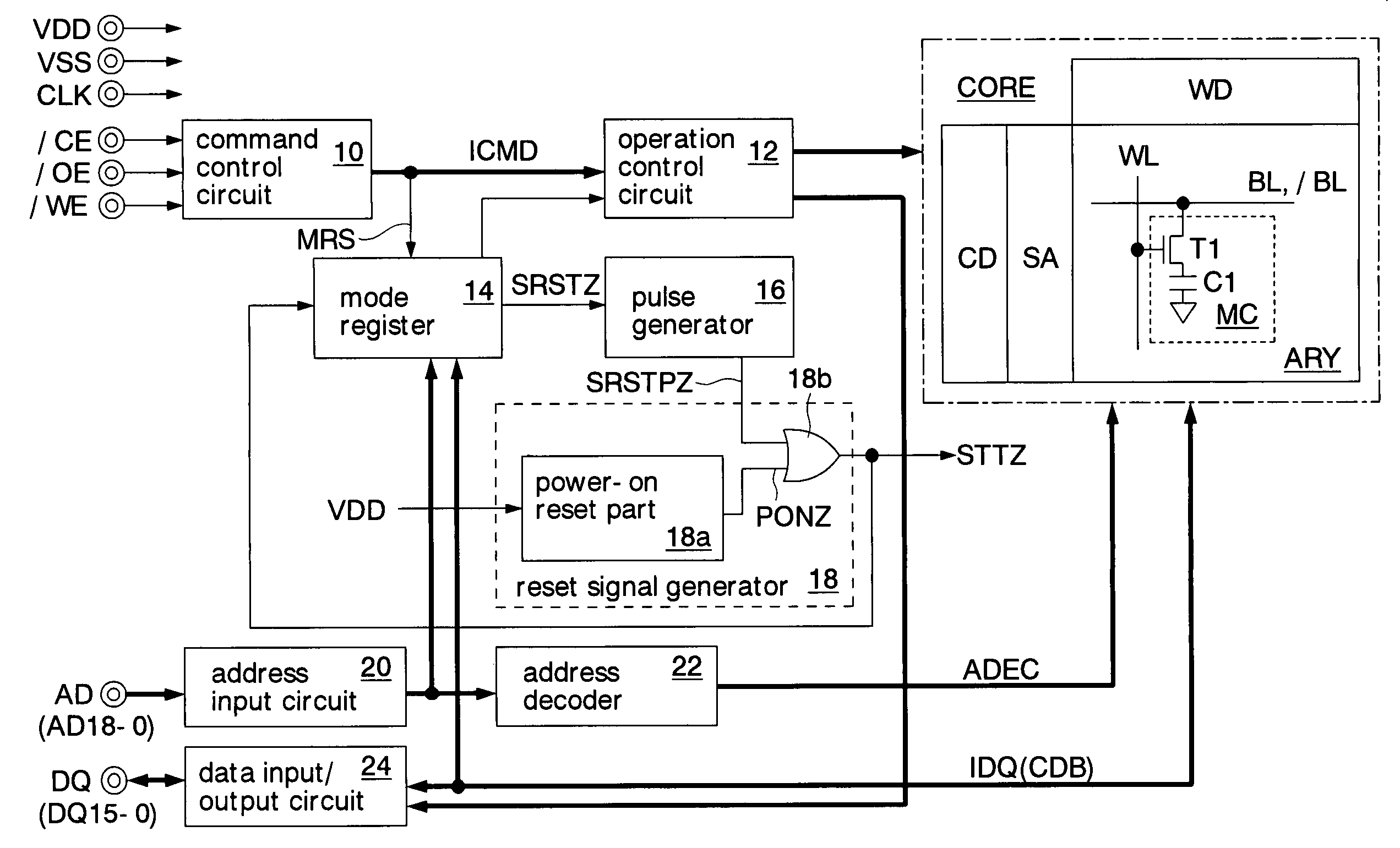
[0028]FIG. 1 illustrates a semiconductor memory according to the present invention. The semiconductor memory is formed as, for example, a fast cycle RAM (FCRAM) using a CMOS process technology. The FCRAM, which has a memory core of a DRAM, is a type of pseudo SRAM having an SRAM interface. The FCRAM has operation modes including a synchronous operation mode that performs a burst operation in synchronization with an external clock CLK, in addition to an asynchronous operation mode such as the SRAM that operates asynchronous to a clock. The FCRAM includes a command control circuit 10, an operation control circuit 12, a mode register 14, a pulse generator 16, a reset signal generator 18, an address input circuit 20, an address decoder 22, a data input / output circuit 24, and a memory core CORE.

[0029] The command control circuit 10 receives a chip enable signal / CE, an output enable signal / OE, and a write enable signal / WE, as external commands, decodes the received external commands, a...

third embodiment

[0060] In the above-mentioned third embodiment, an example where the soft reset pulse signal SRSTPZ is output from the reset output terminal has been described. However, the present invention is not limited thereto. For example, the reset signal STTZ may be output from the reset output terminal.

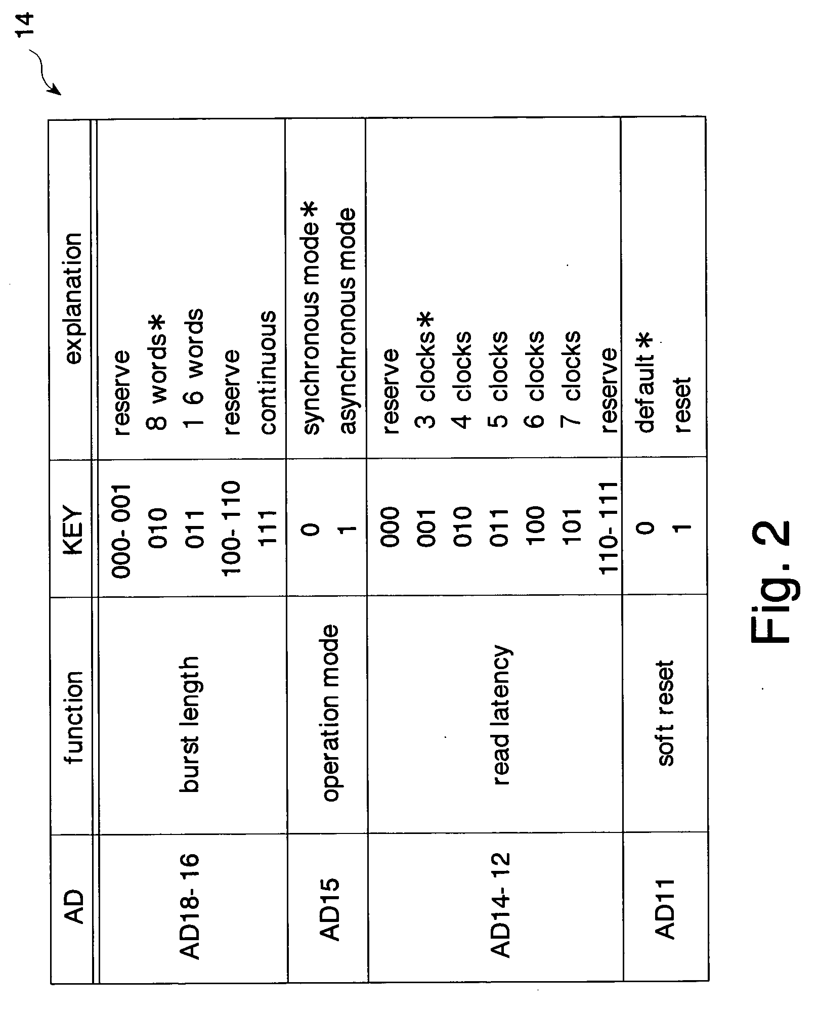
[0061] In the first and second embodiments, examples where each bit of the register part of the mode registers 14 and 14A is set by the external address signal AD have been described. However, the present invention is not limited thereto. For example, the same advantages can be obtained with the external data signal DQ constructed with a number of bits, such as the external address signal AB.

[0062] Moreover, the mode register 14A (FIG. 6) of the second embodiment can be applied to the FCRAM of the first embodiment. Also, the mode register 14 (FIG. 2) of the first embodiment can be applied to the FCRAM of the second embodiment. In addition, The FCRAM of the second embodiment can be applied to...


PUM


Abstract

A register part of a mode register has a plurality of operation setting parts in which plural types of operating specifications are respectively set to operate the semiconductor memory. The mode register outputs a soft reset signal when at least a value of one-bit of the register part represents a reset state. A reset signal generator outputs a reset signal for resetting an internal circuit in response to the soft reset signal. In the present invention, a system that controls the semiconductor memory is required to necessarily assign a predetermined bit with a setting command of the mode register in order to generate the soft reset signal. Accordingly, it is possible to reliably reset the internal circuit by external control.

Description

CROSS-REFERENCE TO RELATED APPLICATION [0001] This application is based upon and claims the benefit of priority from Japanese Patent Application No. 2005-067029, filed on Mar. 10, 2005, the entire contents of which are incorporated herein by reference. BACKGROUND OF THE INVENTION [0002] 1. Field of the Invention [0003] The present invention relates to a semiconductor memory having a mode register that sets an operation mode and a system apparatus having the semiconductor memory mounted thereon. [0004] 2. Description of the Related Art [0005] In general, a semiconductor memory such as a DRAM has a power-on reset circuit. An internal circuit such as a latch is initialized by a power-on reset signal generated when a power supply voltage is low. A method of resetting a test mode register in response to both the power-on reset signal and an initialize command (precharge command) supplied from outside is disclosed in Japanese Unexamined Patent Application Publication No. 11-149771. [0006]...

Claims


Application Information

Patent Timeline
IPC IPC(8): G11C7/00
CPCG11C7/1045G11C11/4072G11C2029/0407G11C7/20G11C11/4076
Inventor NISHIMURA, KOICHIYAMADA, SHINICHINOMURA, YUKIHIRO
Owner SOCIONEXT INC
Why Eureka
Try Eureka