Wafer-processing tape

a processing tape and a technology of dicing tape, applied in the direction of film/foil adhesives, chemistry apparatus and processes, etc., can solve the problems of ics, inferior cutting properties, and easy to cause ics detectives, so as to reduce whisker-like scraps, easy to peel, and good cuttability

Inactive Publication Date: 2006-09-14
FURUKAWA ELECTRIC CO LTD
View PDF7 Cites 50 Cited by
  • Summary
  • Abstract
  • Description
  • Claims
  • Application Information

AI Technical Summary

Benefits of technology

[0026] The wafer-processing tape of the present invention can be applied to a semiconductor wafer, such as a silicon wafer, to use it as a dicing tape when a wafer is diced, and it exhibits such an advantageously effect to reduce whisker-like scraps or the like when the wafer is diced and to make it possible to obtain good cuttability. Further, as a dicing die bond tape, the present invention ensures that the semiconductor element and the adhesive layer can be easily peeled from the removable adhesive layer when wafer chips are picked up, allowing direct die bonding of semiconductor element.

Problems solved by technology

However, the filmy adhesive agent used for these dicing die bond sheets contains a lot of low-molecular-weight material, such as epoxy resins, and tends to be softer than, and inferior in machinability (cutting property) to, a removable adhesive layer used for usual dicing tapes.
This, therefore, has such problems that many whisker-like scraps (swarf) and burrs of the filmy adhesive agent are occurred in dicing; inferior pickup is easily caused in a pickup step after dicing; and, inferior adhesion of chips in a process of fabrication of a semiconductor device, such as ICs, and detectives of, for example, ICs, are easily caused.

Method used


Image

  • Wafer-processing tape
  • Wafer-processing tape

Examples


examples 1 to 8

Comparative Examples 1 to 4

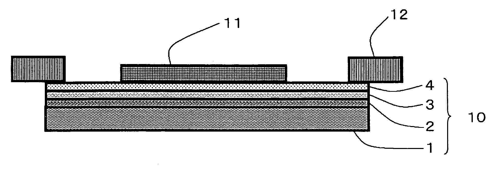
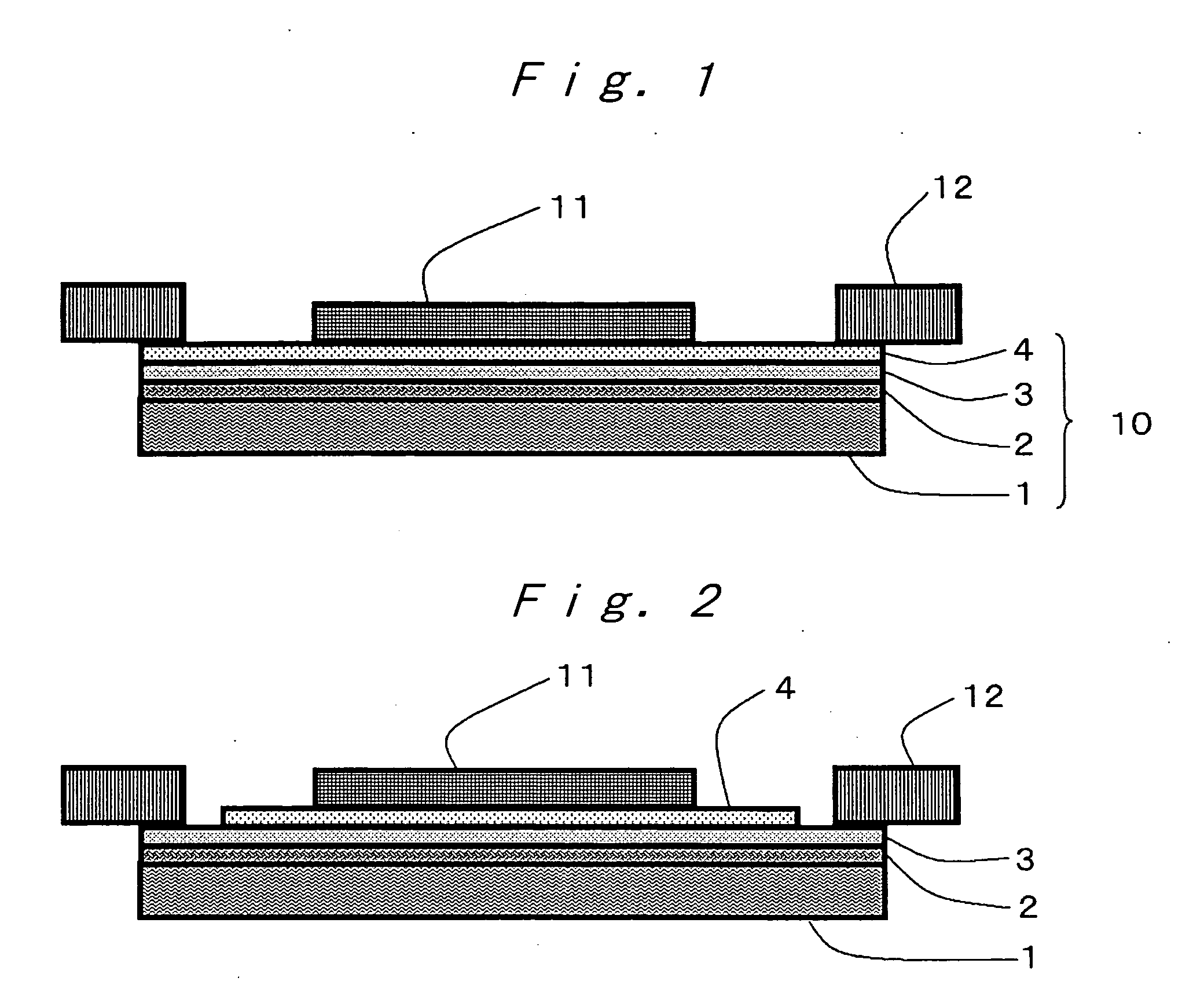
[0089] Each intermediate resin layer composition, removable adhesive layer composition, and adhesive film were prepared in the following manner. Then, onto a 100-μm-thick ethylene / vinyl acetate copolymer film (substrate film), was applied the intermediate resin layer composition so that a dry film thickness would be one, as shown in Table 1, followed by drying at 110° C. for 3 minutes, and then, on the resultant intermediate resin layer, was applied the removable adhesive layer composition so that a dry film thickness would be one, as shown in Table 1, followed by drying at 110° C. for 3 minutes, thereby to produce removable adhesive tapes, respectively. The adhesive film was applied to any one of the removable adhesive tapes such that the adhesive layer would be laminated on the removable adhesive layer, to produce dicing die bond tapes (wafer-processing tapes) of Examples 1 to 8 and Comparative Examples 1 to 4, as shown in Table 1, respectively. The fol...


PUM

PropertyMeasurementUnit
storage elastic modulusaaaaaaaaaa
thicknessaaaaaaaaaa
storage elastic modulusaaaaaaaaaa

Abstract

A wafer-processing tape (10), having an intermediate resin layer (2), a removable adhesive layer (3), and, if necessary, an adhesive layer (4), which are laminated in this order on a substrate film (1), wherein a storage elastic modulus at 80° C. of the intermediate resin layer is larger than a storage elastic modulus at 80° C. of the removable adhesive layer.

Description

TECHNICAL FIELD [0001] The present invention relates to a wafer-processing tape that can be used for processing a wafer, in producing a semiconductor device, such as a silicon wafer. BACKGROUND ART [0002] An assembling process of a semiconductor device, such as an IC or the like, comprises the steps of: cutting and separating (dicing) a semiconductor wafer and the like into respective chips, after patterning; mounting the chips on a substrate or the like; and sealing them with a resin or the like. [0003] In the dicing step, a semiconductor wafer is adhered, and thus fixed, to a dicing die-bond tape in advance, and then it is diced into the shape of chip. In the subsequent mounting step, since an adhesive layer and a removable adhesive layer are configured so that they can peel off from each other, the diced chip to which an adhesive agent is attached, is peeled off (picked up) from the removable adhesive layer, and then fixed, for example, to a substrate by the adhesive agent for ad...

Claims


Application Information

Patent Timeline
Patent Type & Authority Applications(United States)
IPC IPC(8): B32B7/12B32B15/04C09J7/29
CPCB32B7/06Y10T428/28H01L24/27H01L24/29H01L24/83H01L2221/68327H01L2224/274H01L2224/2919H01L2224/83191H01L2224/8385H01L2924/01005H01L2924/01027H01L2924/01033H01L2924/01074H01L2924/01077H01L2924/01078H01L2924/01082H01L2924/07802H01L2924/14H01L21/6836Y10T428/2891Y10T428/2848H01L2924/00013H01L2924/0665H01L2924/01023H01L2924/01019H01L2924/01006H01L2224/29298H01L2224/29H01L2924/00H01L2924/00014H01L2924/3512H01L2224/29099H01L2224/29199H01L2224/29299H01L2224/2929H01L2924/12042C09J7/29C09J2203/326C09J2301/122C09J2301/162C09J2433/006H01L21/48
Inventor KITA, KENJIMORISHIMA, YASUMASAISHIWATA, SHINICHIYABUKI, AKIRA
Owner FURUKAWA ELECTRIC CO LTD
Why Eureka
Try Eureka