Display device

a display device and circuit technology, applied in the direction of instruments, cathode ray tubes/electron beam tubes, electric discharge tubes, etc., can solve the problems of generating brightness irregularities, increasing power consumption of data drivers which constitute modulation circuits for driving longitudinal lines, so as to prevent the generation of deterioration of image quality, reduce the operation of sum of products, and high image quality

Inactive Publication Date: 2006-09-21
HITACHI DISPLAYS
View PDF0 Cites 25 Cited by
  • Summary
  • Abstract
  • Description
  • Claims
  • Application Information

AI Technical Summary

Benefits of technology

[0026] A sum-of-product operation within one horizontal scanning period becomes a sum-of-product operation of N×N for calculating the total electric current. Compared to the conventional method described in patent document 1 in which the sum-of-product operation of N×N is performed N times, the sum-of-product operation can be drastically reduced by 1 / N times.
[0027] Further, from the output point of the scanning circuit to the electronic emission element which is arranged at the end portion of the horizontal line, it is possible to compensate for the voltage drop attributed to the resistance of the horizontal line.
[0028] Still further, even when the resistance of the horizontal line differs for every line due to the line arrangement or the like from the output point of the scanning circuit to the electronic emission element which is arranged at the end portion of the horizontal line, it is possible to prevent the generation of the deterioration of image quality.
[0029] As has been described above, according to the display device of the invention, it is possible to realize the high image quality and the low-power-consumption characteristics. Still further, since the number of sum-of-product operations can be reduced, the sum-of-product operations can be performed with a simple hardware.
[0030] According to the display device of the invention, it is possible to realize the high image quality characteristics which exhibit the small correction error and the light emitting time with a little signal dependency.
[0031] Further, according to the display device of the invention, the output of the differential amplifier can be stabilized thus preventing the generation of irregularities of the images.

Problems solved by technology

Accordingly, a voltage drop is generated in horizontal line which is connected to the upper electrode thus generating brightness irregularities.
However, in the MIM type electron emission element, a parasitic capacitance of the longitudinal line is large and hence, there has been a drawback that due to the increase of an amplitude of the longitudinal line voltage attributed to the voltage correction, the power consumption of a data driver which constitutes a modulation circuit for driving the longitudinal line is increased.
Further, in the above-mentioned patent document 3 (Japanese Patent 3311201), the voltage drop correction attributed to the output ON resistance of the scanning circuit is performed by the voltage correction of a pulse which is outputted to the longitudinal line and hence, as described previously, there arises a drawback that due to the increase of an amplitude of the longitudinal line voltage attributed to the voltage correction, the power consumption of a data driver which constitutes a modulation circuit for driving the longitudinal line is increased.
Further, these patent documents also fail to take the correction of voltage drop which is generated due to the output ON resistance when a scanning circuit is formed on both sides of a display panel and the same horizontal line is simultaneously driven from both sides into consideration.

Method used


Image

  • Display device
  • Display device
  • Display device

Examples


embodiment 1

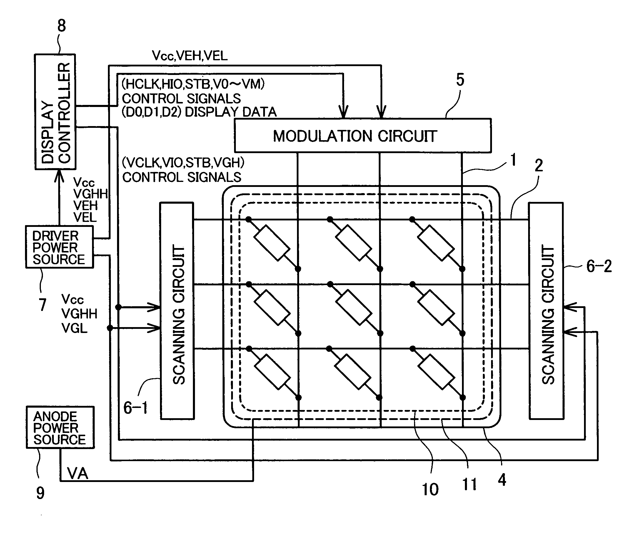
[0057]FIG. 1 is a block diagram showing the whole circuit constitution (1) of this embodiment. A display panel 4 includes a back plate, a face plate and a side wall (not shown in the drawing). The back plate includes longitudinal lines 1 which extend in the longitudinal direction (Y direction), horizontal lines 2 which extend in the lateral direction (X direction), and each electron emission element 3 which is connected to one longitudinal line and one horizontal line. A plurality of longitudinal lines is arranged in the lateral direction, while a plurality of horizontal lines are arranged in the longitudinal direction. An MIM type electron emission element can be used as the electron emission element. The face plate includes phosphor films 10 and a metal back 11 which is formed to cover the phosphor films 10. A surface of the face plate on which the electron emission elements 3 are formed and a surface of the back plate on which a phosphor screen is formed face each other in an opp...

embodiment 2

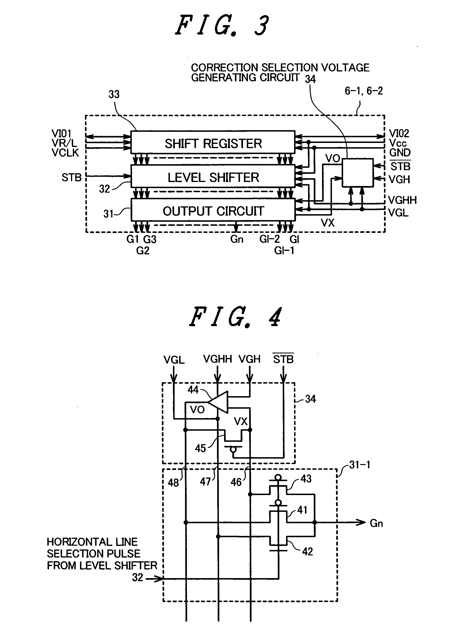
[0117] The above-mentioned embodiment 1 is directed to the case in which the overshooting is generated when the output voltage Gn of the output circuit rises from the non-selection voltage VGL to the selection voltage VGH and hence, the high accuracy control of the light emitting amount is difficult.

[0118] This overshooting is generated based on a phenomenon that the input voltage change is delayed with respect to the output voltage change of the differential amplifier 44 due to the delay attributed to the ON resistance of the pMOS selection switch 41 and the line capacitance of the horizontal line 2 or the delay attributed to the pMOS detection switch 43 and the line capacitance of the input line 46 of the differential amplifier 44.

[0119] In this embodiment, the OFF time of the pMOS feedback switch 45 is delayed than the ON time of the pMOS selection switch41 and the pMOS detection switch 43 of the selected horizontal line.

[0120]FIG. 8 shows the output timing of the data driver ...

embodiment 3

[0126] In this embodiment, the data driver output voltage is corrected by taking the resistance Ro2 to pixels at both ends from the output point of the scanning driver into consideration in Embodiment 2. FIG. 9 is a view for explaining the horizontal line voltage drop and the manner of correction at such a point of time.

[0127] In FIG. 9, symbols 3, r, Ro, im are substantially equal to the corresponding symbols shown in FIG. 6, while symbols iRm′, iLm′, Vm′, Im′, VVL′, VVR′ are substantially equal to the corresponding symbols iRm, iLm, Vm, Im, VVL, VVR shown in FIG. 6. Further, symbol Ro2 indicates the resistance from the scanning driver output point to the pixels at both ends.

[0128] The horizontal line voltage drop Vm′ generated in the mth pixel is obtained as follows. By inputting corrected values VVL′ and VVR′ respectively to the scanning driver output circuits, the amount of voltage drop at the output points of the scanning drivers become zero and hence, the left and right outp...


PUM


Abstract

A display device of the invention includes horizontal lines, longitudinal lines, electron emission elements, and a scanning circuit which performs the selection of the horizontal lines. The scanning circuit includes a non-selection voltage switch, a correction selection voltage switch, and an output voltage detection switch for the selected horizontal line for every horizontal line. The display device also includes a differential amplifier which is connected to a correction selection voltage input line, a horizontal line selection voltage line, and a correction selection voltage output line for every plurality of horizontal lines. The invention can suppress a voltage drop of the horizontal lines and, at the same time, can suppress the brightness irregularities of the display device.

Description

CROSS-REFERENCE TO RELATED APPLICATION [0001] The present application claims priority from Japanese application JP2005-073142 filed on Mar. 15, 2005, and Japanese application JP2005-072779 filed on Mar. 15, 2005, the content of which is hereby incorporated by references into this application. BACKGROUND OF THE INVENTION [0002] 1. Field of the Invention [0003] The present invention relates to a scanning circuit which performs the selection of scanning lines of display panel having a particularly of scanning line (horizontal line) and a plurality of longitudinal line. [0004] The present invention relates to a display device which is capable of correcting a voltage drop in a scanning line (horizontal line), and more particularly to a display device which uses MIM type electron emission elements. [0005] 2. Description of the Related Art [0006] Heretofore, as a cold cathode electron emission element, there has been known a metal / insulator layer / metal type electron emission element (herei...

Claims


Application Information

Patent Timeline
Patent Type & Authority Applications(United States)
IPC IPC(8): G09G1/04
CPCG09G3/22G09G2310/0267G09G2320/0204G09G2330/02G09G2330/021
Inventor OZAKI, TOSHIFUMITSUKAHARA, MASAHISAMISONOU, TOSHIKI
Owner HITACHI DISPLAYS
Why Eureka
Try Eureka