

Substrate processing apparatus
a substrate processing and plasma technology, applied in the direction of coatings, chemical vapor deposition coatings, electric discharge tubes, etc., can solve the problems of difficult complete removal of deposits, serious problems, unstable substrate processing, etc., and achieve the effect of suppressing problems
- Summary
- Abstract
- Description
- Claims
- Application Information
AI Technical Summary
Benefits of technology
Problems solved by technology
Method used
Image

Examples
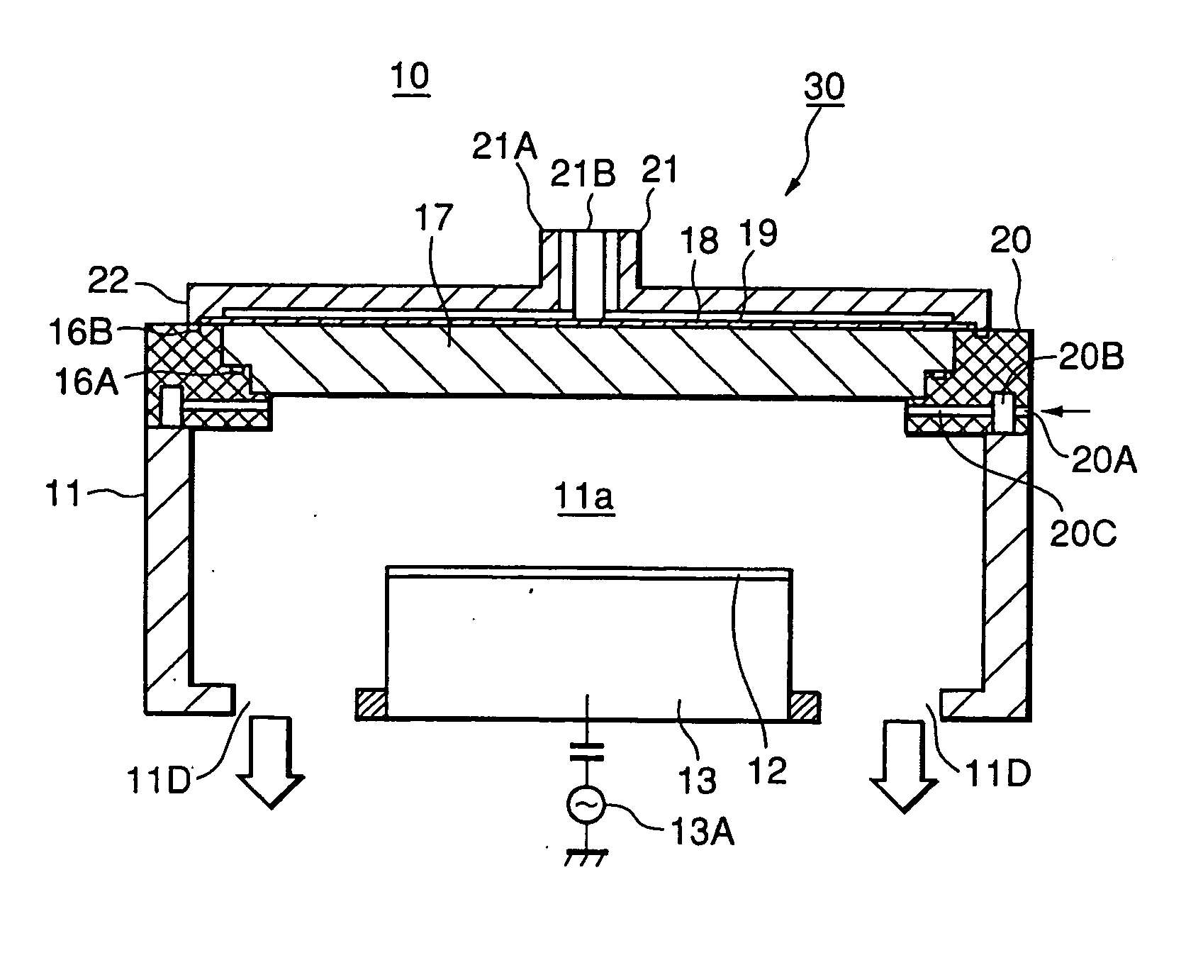
first embodiment
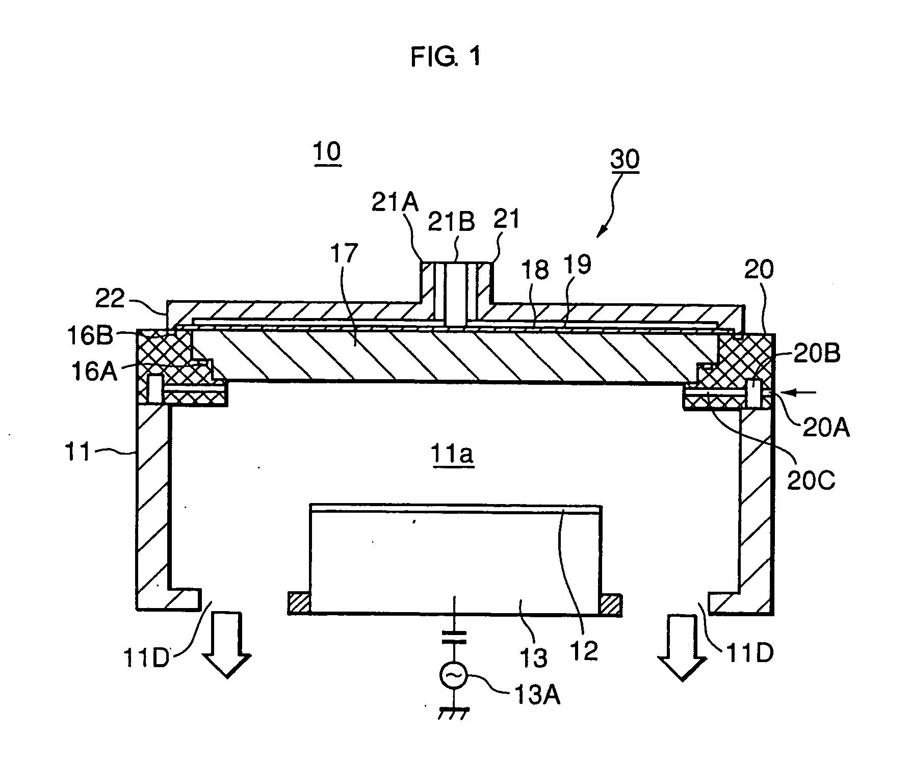
[0039]FIG. 2 shows a structure of a plasma processing apparatus 10A being a substrate processing apparatus according to a first embodiment of this invention. In the figure, the same reference symbols are assigned to those portions that have been described before in FIG. 1, thereby omitting description thereof.
[0040] Referring to FIG. 2, in the plasma processing apparatus 10A, a plasma gas supply ring 14 for introducing a plasma gas into the processing chamber 11 is inserted between the microwave transmissive window 17 and the processing chamber 11 so as to define the outer wall of the processing chamber 11 and, further, an approximately cylindrical inner partition wall 15 is attached to the plasma gas supply ring 14. The inner partition wall 15 is engagingly attached to a partition wall attaching portion of the plasma gas supply ring 14 and the microwave transmissive window 17.
[0041] The space in the processing chamber 11 is divided by the inner partition wall 15 into 11A being a ...
second embodiment
[0049]FIG. 3 is a perspective view of the inner partition wall 15. In the figure, the same reference symbols are assigned to those portions described before, thereby omitting description thereof.
[0050] It is configured that the inner partition wall 15 is made of the approximately cylindrical conductor, for example, the stainless alloy and the heater 15B is attached onto its side facing the outer wall of the processing chamber 11 so that it is possible to heat the inner partition wall 15.
[0051] The inner partition wall 15 is formed at its end portion with the plasma gas supply holes 15A for allowing the plasma gas supplied from the plasma gas holes 14C to pass therethrough so as to be supplied to the space 11A.
[0052] The plasma gas supply holes 15A are configured so as to correspond to the plasma gas holes 14C formed in the plasma gas supply ring 14 when the inner partition wall 15 is attached to the plasma gas supply ring 14 so that the plasma gas is supplied to the space 11A fro...
third embodiment
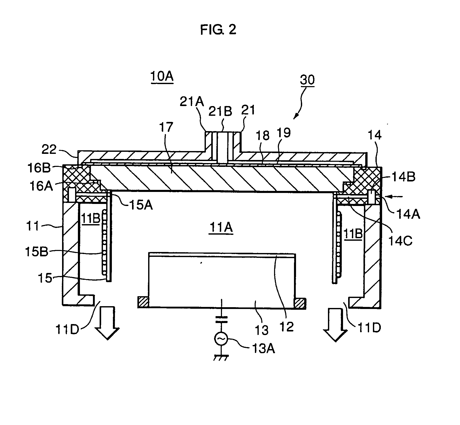
[0055] FIGS. 4(A) and 4(B) show the plasma gas supply ring 14, wherein FIG. 4(A) is a plan view and FIG. 4(B) is a sectional view taken along A-A shown in FIG. 4(A).
[0056] Referring to FIGS. 4(A) and 4(B), the plasma gas supply ring 14 has an approximately disk shape formed with a center space 14F such that the space 14F forms part of the space 11A when the plasma gas supply ring 14 is installed in the plasma processing apparatus 10A.
[0057] It is configured that, as described before, the plasma gas supply ring 14 is formed with the stepped shape from its side facing the space 14F toward its peripheral portion so that its stepped shape engages the stepped shape of the microwave transmissive window 17.
[0058] Further, an approximately ring-shaped ring groove 14E for insertion of the seal ring 16A is formed at the stepped shape portion of the plasma gas supply ring 14 on the side facing the microwave transmissive window 17. The seal ring 16A is inserted into the ring groove 14E so th...
PUM
| Property | Measurement | Unit |
|---|---|---|
| Current | aaaaa | aaaaa |
| Current | aaaaa | aaaaa |
| Digital information | aaaaa | aaaaa |
Abstract
Description
Claims
Application Information