High density semiconductor memory and method of making
- Summary
- Abstract
- Description
- Claims
- Application Information
AI Technical Summary
Problems solved by technology
Method used
Image

Examples
Embodiment Construction
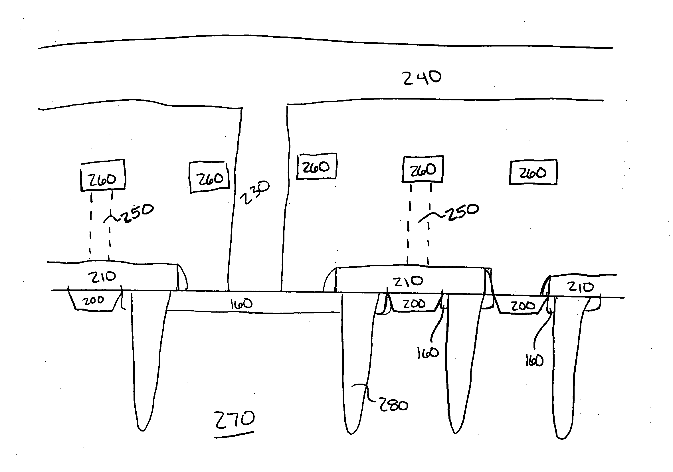
[0034] An exemplary embodiment of an arrangement of active areas of an array of memory cells according to the present invention is depicted in FIG. 2. A plurality of cross-shaped active areas 160 are arranged with each succeeding cross-shaped active area 160 offset by 4 F in the x direction and 2 F in the y direction. Each cross-shaped active area 160 is depicted as having four arms 165 extending from a body portion 166. The body portion has an area of 1 F2, and each arm 165 has a width of 1 F, and a length of 2 F. Each arm 165 is positioned at approximately a 90° angle from each of the two adjacent arms 165.
[0035] The cross-shaped active areas 160 are packed more densely than the active areas of a conventional array of memory cells, and each cross-shaped active area 160 is shared by four cells. Each cell includes a capacitor, or storage node 180, represented with a “+” and positioned at a distal tip 167 of each active area arm 165. It is noted that the term “capacitor” as used her...
PUM
 Abstract
Description
Claims
Application Information